Two weeks ago, I travelled to Prague in the Czech Republic, where more than 1400 scientists had descended on the city for one of the biggest events in the particle-physics calendar. I was attending the International Conference on High Energy Physics (ICHEP), which takes place every two years and attracts scientists from all over the world.
Almost 1000 parallel talks were crammed into the first three days of the week-long conference, and with 13 parallel sessions, I kept myself fit running between floors to catch everything I wanted to see. I tried to see a bit of everything, from Higgs physics to neutrinos and from future colliders to cosmology.
As well as presentations of scientific results, the event featured discussions about equality diversity and inclusion (EDI), education and outreach, all relatively new additions to the conference programme.
This was also the first ICHEP with a dedicated stream on sustainability. I spoke to Jorgen D’Hondt, a professor at Vrije University Brussels, who delivered a presentation about the “Innovate for Sustainable Accelerator Systems” project. Climate change has brought energy consumption to the forefront of all our minds and particle physics is no exception. D’Hondt argued that particle physicists have a responsibility to make their experiments, many of which will operate decades into the future, as efficient as possible.
“I don’t think people in the 2040s will ask us whether we are using green energy. Because by that time most of the energy will be green” said D’Hondt. “I believe the question of that generation will be can we as scientists demonstrate that our facilities have done all they can to reduce our energy footprint.”
After three hectic days of parallel sessions, I was grateful that the second half of the conference gave me a chance to rest my feet. We settled into a huge theatre for the plenary talks, which were longer than the parallel sessions, but each speaker still had the difficult task of condensing several years of research in their field into a 25-minute slot.
When I was asked by attendees what I was doing at ICHEP, my stock answer was that I was there to discover where the next big discovery – on a par with the Higgs boson – will come from. It’s no surprise therefore that my ICHEP highlight was a panel debate on future colliders.
From dark energy to the asymmetry between matter and antimatter, we’ve discovered that the standard model has some serious limitations, and the search is on for new physics. The big question for the panel was where, and who, this will come from.
From what I saw, the frontrunner experiment is undoubtably a “Higgs factory”. Higgs bosons have been linked to many of the puzzling gaps in the Standard Model of particle physics and a Higgs factory is a collider that would produce them at a high rate, allowing their properties to be measures with great precision.
All the organizations represented on the panel have expressed interest in building such an experiment, and Wang was particularly optimistic about China’s ability to follow through on their proposal, the Circular Electron Positron Collider (CEPC), saying “we have a mission to be one of the world leaders in particle physics”.
He also acknowledged that this could put IHEP in competition with CERN, which has its own proposal for a similar experiment called the Future Circular Collider (FCC). Perhaps the elephant in the room during this discussion was the impact that future diplomatic relations, particularly between the US and China, could have on these collider projects – something that came up frequently in other discussions during the conference.
Not everyone I spoke to was convinced that the Higgs factory should be prioritized by the field, and I saw many innovative proposals for smaller experiments. What makes particle physics so exciting is that while we’re pretty sure new physics is out there, no-one knows for sure where we should be looking for it.
While some are impatient for another big break, it’s only been 12 years since the discovery of the Higgs boson – a relatively short time in a field that is always looking several decades into the future. I’ll be keeping a watchful eye for big decisions in the next few years, as high-energy physics finds its next steps.
This episode of the Physics World Weekly podcast features an interview with Margaret Arakawa. She is chief marketing officer at IonQ – which makes trapped ion quantum computers. An economist by training, Arakawa spent 25 years in the (classical) computing industry before joining IonQ. We chat about why she made the move to the quantum sector and about the wide range of opportunities for non-physicists in the quantum-technology industry.
Arakawa also talks about the challenges of marketing quantum technology to customers who might not understand the underlying physics and explains why the quantum industry must avoid hype.
Our second guest is Nat Mendelsohn, who represents the English Midlands on the Institute of Physics’ Student Community Panel. He talks to Physics World’s Katherine Skipper about the student experience – what is good and what can be improved. He also explains how the COVID-19 pandemic continues to have a profound impact on higher education.
Finally, I chat with Skipper about her trip to Prague for the 42nd International Conference on High Energy Physics. High on the agenda was what collider of the future will be the successor of the Large Hadron Collider.
A quantum computing system that uses the spins of holes in germanium quantum dots has been unveiled by researchers in the Netherlands. Their platform is based on a 1998 proposal by two pioneers of quantum computation theory and could offer significant advantages over today’s technologies.
Today, the leading platforms for quantum bits (qubits) are superconducting quantum circuits and trapped ions, with neutral atoms trailing slightly behind. However, all of these qubits are difficult to scale-up and integrate to create practical quantum computers. For example IBM’s Condor – perhaps today’s most powerful quantum computer – uses 1121 superconducting qubits. These must all be kept at millikelvin temperatures, and as the number of qubits grows towards the tens of thousands or even millions, the energy cost and engineering challenges of keeping processors cold become daunting. Other platforms present other scaling challenges that are as significant.
Quantum dot qubits were proposed in 1998 by Daniel Loss of the University of Basel and David DiVicenzo, then at IBM. The qubit state is defined by the quantum state of a single charge on a semiconductor quantum dot, and shuttling the charge between quantum dots allows quantum gate operations to be performed. These systems would need less cooling, and they could potentially be fabricated in semiconductor foundries.
Quantum well
Menno Veldhorst of QuTech in the Netherlands, who co-led this latest research, describes the architecture of the quantum dots. “First, we have a semiconductor heterostructure,” he explains, “This is layers of silicon, silicon–germanium and germanium in our case. And then we have a 2D sheet of germanium, which is the quantum well that we’re interested in. We can confine charges in that 2D sheet, which is maybe 60 nm thick. And then we have electric gates on top so that, if we apply a voltage to those gates, we can define a potential well in which single charges can be trapped.”
In principle, this is a very attractive design, creating a transistor that is a qubit. In practice, however, it has been very difficult to achieve. Loss and DiVicenzo originally envisaged a series of adjacent quantum dots, all subject to different magnetic fields.
“If you have two quantum dots and you put a charge in one of them it will go to its ground state,” says Veldhorst. “If I want to do a qubit operation, say rotating the spin, I can flip it to another quantum dot. But in the other quantum dot, the ground state will be pointing in a different direction. What happens as a result is that the qubit starts to make oscillations as it precesses around this new quantization axis. If I wait a certain amount of time and then pop back to the original dot, I may have flipped the spin state completely.” This procedure would allow arbitrary qubit rotations to be performed with simple applied voltages.
The challenge is creating different magnetic fields on adjacent quantum dots. For the past two decades groups such as Veldhorst’s have applied high-frequency oscillating external magnetic fields to manipulate the spins of electrons, usually in silicon, as they move between quantum dots. These fields increase the power requirements and add noise.
Spin-orbit interaction
In the new work Veldhorst and colleagues looked at Loss’s idea of using holes – quasiparticles created by the absence of electrons – instead of electrons. Like electrons, holes have an energetic coupling to an external magnetic field, giving rise to two distinct energy levels that can create a qubit. However, holes have a much stronger spin-orbit interaction, in which the momentum of the hole is coupled to its spin. Furthermore, this interaction varies between quantum dots.
The team used holes in their germanium quantum dots. By simply applying a static magnetic field of 40 mT and megahertz-frequency electric fields, the researchers were able to execute quantum logic with single-qubit gate fidelities of 99.97% and two-qubit gate fidelities of 99.3%. Their principal problem today is that they cannot control the anisotropy of the quantum dots. Veldhorst explains that researchers normally try to make quantum dots perfect circles, and their next step will be to make them slightly elliptical to introduce this anisotropy. “This is another thing that, on paper, sounds nice, but whether it will be the case we don’t know,” he says; “But I think we’ve opened a new direction of research with a lot of possibilities.”
Theorist Edwin Barnes of Virginia Tech in the US believes the work is, “a pretty major advance in this area of quantum computing. In the past 20 years people have focused on applying microwaves to perform operations on the qubits, rather than doing this hopping which was in Loss and DiVicenzo’s original paper. In this recent [work] they’re showing that this hopping idea works, and that it seems to work extremely well.” He believes the stochastic variation of the magnetization between quantum dots should not prove insurmountable, as “it just means you just have to spend longer characterizing your device before you start using it”. The next step, he believes, is scaling up.
In 2022, more than 10.5 million people fell ill with tuberculosis (TB) and an estimated 1.3 million people died from this curable and preventable disease. TB is currently diagnosed using clinical evaluations and lab tests. While spit (sputum) tests and chest X-rays are common, a physician may also recommend a PET scan.
Current PET scans use radiotracers that could indicate TB or other diseases. A PET scan that targets TB bacteria specifically could enable more effective treatment, say researchers at the Universities of Oxford and Pittsburgh, the Rosalind Franklin Institute and the NIH.
“TB normally requires quite long treatment regimens of many months, and it can be tricky for patients to stay enrolled in these,” explains Benjamin Davis, science director for next generation chemistry at the Rosalind Franklin Institute and a professor of chemical biology at the University of Oxford. “The ability now to readily track the disease and convince a patient to stay engaged and/or for the physician to know that treatment is complete we think could prove very valuable.”
Davis and his team have developed a radiotracer, called FDT (2-[18F]fluoro-2-deoxytrehalose), that is taken up by live tuberculosis bacteria. FDT-PET scans show signal where tuberculosis bacteria are active in a patient’s lungs and measure the metabolic activity of the bacteria, which should decrease as a patient receives treatment.
“We came up with a way of designing a selective sugar for tuberculosis by understanding the enzymology of the cell wall of TB,” Davis says. “Specifically, we target enzymes in the cell wall that modify FDT, so that it effectively embeds itself selectively into the bacterium. If you like, this is a sort of self-painting mechanism where we get the pathogen to use its own enzymes to modify FDT and so ‘paint itself’ with our radiotracer.”
The researchers have characterized FDT and tested the radiotracer in preclinical trials in rabbits and non-human primates. Phase I clinical trials in humans are set to begin in the next year or so. “We are in the process of identifying partners and sites as well as addressing the differing modes of trial registration in corresponding countries,” says Davis.
Another benefit of FDT is that it can be produced from FDG – a common PET radiotracer – without specialist expertise. FDT could thus be a viable option in low- and middle-income countries with less developed healthcare systems, the researchers say, though it does require that a hospital have a PET scanner.
Writing in a press release, Clifton Barry III from the National Institute of Allergy and Infectious Diseases at the NIH, says: “FDT will enable us to assess in real time whether the TB bacteria remain viable in patients who are receiving treatment, rather than having to wait to see whether or not they relapse with active disease. This means FDT could add significant value to clinical trials of new drugs, transforming the way they are tested for use in the clinic.”
Every year one early-career researcher who’s made “exceptional contributions to experimental physics” is awarded the Henry Moseley medal and prize from the Institute of Physics (IOP). In 2023 the medal was given to Hannah Stern for her work on understanding the photophysics of semiconductors and 2D materials. As of January, Stern is an assistant professor at the Photon Science Institute at the University of Manchester, UK. She was previously a research fellow at the University of Cambridge, where she also obtained her PhD in 2017.
Stern’s group is developing new platforms for quantum technologies, with a focus on materials with quantum states that can be controlled with light. She recently led research with colleagues in the UK and Australia which showed that lattice point defects in hexagonal boron nitride (hBN) have promising properties for quantum technologies, including sensing and optical networking (Nature Materials 10.1038/s41563-024-01887-z).
Katherine Skipper caught up with Stern to discover what motivates her research, what the big challenges facing the quantum sector are, and what the ethos of her new group will be.
What first sparked your interest in quantum technology?
I’ve always been intrigued by quantum mechanics. When I was an undergraduate at Otago University in New Zealand, I majored in physical chemistry, and I gained experience with spectroscopic techniques. In these experiments, we would shine light at materials and use the data we collected to understand the electronic structure of those materials on the atomic and molecular level. I found this exciting because it felt like I could really see quantum mechanics at work.
I continued with different forms of spectroscopy for my PhD and learnt a lot more about electronic spin states in materials that could be generated via light. I didn’t start thinking about the implications of these systems for quantum technologies until later. As a postdoc, I became interested in states in materials that emit single photons at a time. That was when I realized that the physics I had been studying had applications within quantum technology.
Your research is on light–matter interfaces for quantum technologies. Why is the interaction between light and matter important for quantum applications?
Understanding the interaction between light and matter has always been central to building our understanding of quantum mechanics. Today, light–matter interactions on the single particle level are one of the most useful ways to control and use quantum phenomena for new technologies.
In the first instance, quantum technologies require qubits, which are the quantum equivalent of the classical bit. In simple terms, a qubit is a two-level system that can exist in a quantum superposition state. Qubits can be formed not only from electronic and magnetic transitions within materials but also from single photons. Both form of qubits are being actively developed for different applications.
While light and matter qubits can be used separately for quantum technologies, we can get new functionality by harnessing the interaction between them
For example, photons are useful for applications that require transportation of quantum states (i.e. for communication technologies) because they can be sent long distances without losing quantum information, which may be encoded in the photon polarization, for example. Qubits in matter, however, such as electronic or nuclear spins, are often better at storing information for longer periods of time. Typically, they can also be controlled more easily than photons so they are more suitable for performing logical operations on the device level, for example in computing or simulation.
What this means is that while light and matter qubits can be used separately for quantum technologies, we can get new functionality by harnessing the interaction between them. A good example is “quantum optical networks”. Long-distance optical quantum networks don’t exist yet, but it could enable a quantum version of the internet, in which quantum information is distributed across a series of globally positioned nodes.
These nodes could be material qubits, which would send and receive quantum information from photons and store it locally as a quantum memory. As it turns out, a promising material system for this is atomic-scale point defects in materials, which is what I work on.
What kind of qubits in matter do you study? And how does the interaction with light enable these systems?
Qubits in matter often come in the form of electronic or nuclear spin transitions of atoms or molecules – what are called “spin qubits”. Spin is one of the non-intuitive concepts of quantum mechanics that doesn’t have a classical analogue – it refers to an intrinsic property (angular momentum) of a particle. Importantly, spin is quantized, meaning particles can only exist in a limited number of possible spin states.
What’s interesting about the spin qubits I work with is that the state of the qubit can be controlled with light
The simplest example is the spin state of a single electron, which can be spin up, spin down or a superposition of those two states. Often the spin state of an atom, defect or molecule is slightly more complex – in fact, the materials I work with are an example of this. But it’s typically still possible to think about the spin state in this way.
What’s interesting about the spin qubits I work with is that the state of the qubit can be controlled with light. We first use a laser pulse to place the qubit into a useful spin state before manipulating it with a second electromagnetic pulse and using a second laser pulse to “read-out” the new state. Known as optically detected magnetic resonance, it forms the basis of how we use the spin qubit to store quantum information or sense the environment.
The systems I work with are formed from atomic-scale point defects in an extended solid, in this case a 2D material. You could think of these defects as a missing atom in the lattice. The disruption of the lattice creates a “trapped molecule” in the crystal, which is electronically isolated and has well defined electronic transitions between optical and spin states, forming a qubit.
One appealing feature of defects in solids for quantum applications is that they work at ambient conditions, without needing low temperatures or high magnetic fields. The spin control pulse in our experiments is generally in the microwave or radio range, which is good because we can easily implement microwave or radio frequency control on a chip, and at room temperature. It’s quite hard to find other isolated quantum objects that can be manipulated at ambient conditions.
What are the applications of spin qubits?
In addition to optical networking applications, one important application is in sensing. Most sensors measure a physical quantity over a bulk, or spatially averaged, sample. An exciting feature of sensors based on single electronic spins is that the sensor itself is now atomic scale and can measure physical quantities with very high (near atomic-scale) spatial resolution.
One particularly active area of quantum sensing right now is quantum nanoscale magnetometry
One particularly active area of quantum sensing right now is quantum nanoscale magnetometry, which exploits the fact that an external magnetic field will shift the energy of the electronic spin states of a spin qubit.
By measuring the energy shift of the spin states (via optically detected magnetic resonance), we can work out the magnitude and direction of the field at a precise point in space. So by scanning the qubit over a sample, the nanoscale magnetism of materials can be visualized in a way that has not been possible before.
What kinds of materials have spin properties that can be used in quantum technologies?
Several factors determine if a material will be useful for quantum technologies, and they also depend on the technology you are talking about. Typically, if a material that hosts spin qubits is going to be useful for a quantum application, it needs to have a significant spin coherence time, which is how long a spin can hold on to quantum information.
For sensing, generally the longer the coherence time the more sensitive the sensor. For optical networking, the spin coherence time limits how far the photon can be sent in the network. For both applications, typically a coherence time of at least milliseconds is desirable.
The coherence time of a spin qubit can be limited by a range of environmental factors. For solid-state spin qubits based on defects, the most common limitation is magnetic noise from neighbouring nuclear spins and electronic impurities. This means that the spin needs to be isolated, so we typically use materials with a low abundance of spin-active nuclei. Diamond is well known for this.
You’ve recently investigated the spin properties of defects in hBN: what makes it attractive for quantum applications?
hBN is a 2D material with a wide band gap. Because it’s an insulator, we wouldn’t expect it to interact with visible wavelengths of light, but in about 2016 localized emission of visible light was observed in a hBN lattice (Nature Nanotechnology 11 37).
The idea was put forward that this emission comes from atomic-scale defects in the lattice. By the time I got interested, quite a lot of work had been done to optically characterize the defects, but we didn’t know whether this optical transition could interact with an electronic spin state of the defect.
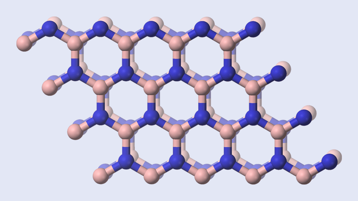
Material idea Hannah Stern and her group are looking at the spin properties of defects in hexagonal boron nitride, which is a 2D material and has promise for quantum applications. (Public domain)
At that point, there was the nitrogen-vacancy centre in diamond and a couple of other defects in silicon carbide, but not many other defects in materials that offered optically addressable electronic spin qubits.
In our most recent paper, we’ve shown that there are spin states of these defects that we can initialize, control and then read out using light. And these defects can store quantum information for microseconds at room temperature.
In addition, many spin qubits require a magnetic field to operate, either to initialize the qubit or to separate the spin qubit transitions from other electronic transitions. Here however, we can control the spin without any magnetic field. While the coherence times are still relatively short compared to other systems, this is all being performed under ambient conditions and in a brand new material platform.
This is also the first time spin defects with these properties have been studied in a layered material as opposed to a bulk crystal. 2D materials offer natural advantages for fabrication because they can be easily moved from surface to surface and incorporated with other materials and optical components, such as wave guides or cavities, that we may like to use in future to improve the collection of light from the defects. It can be extremely challenging to couple photons coming from the middle of a crystal to such components.
All of these things are quite exciting because they speak to this type of physics being available in a device that might operate in real world conditions.
What further work is needed to take hBN out of the lab and into real-world devices?
We have a lot to do. We’re interested in technologies that use both the spins and the photons of the hBN defects, and while we’ve made some strides in understanding the spin physics, we’ve got a lot more to understand on the optical properties. A big challenge before us is identifying the chemical structure of the defect. We believe it’s related to carbon inserted in the lattice but we don’t know the exact arrangement of the carbon atoms in the hBN lattice and that’s what we’re working hard to determine in collaboration with theorists.
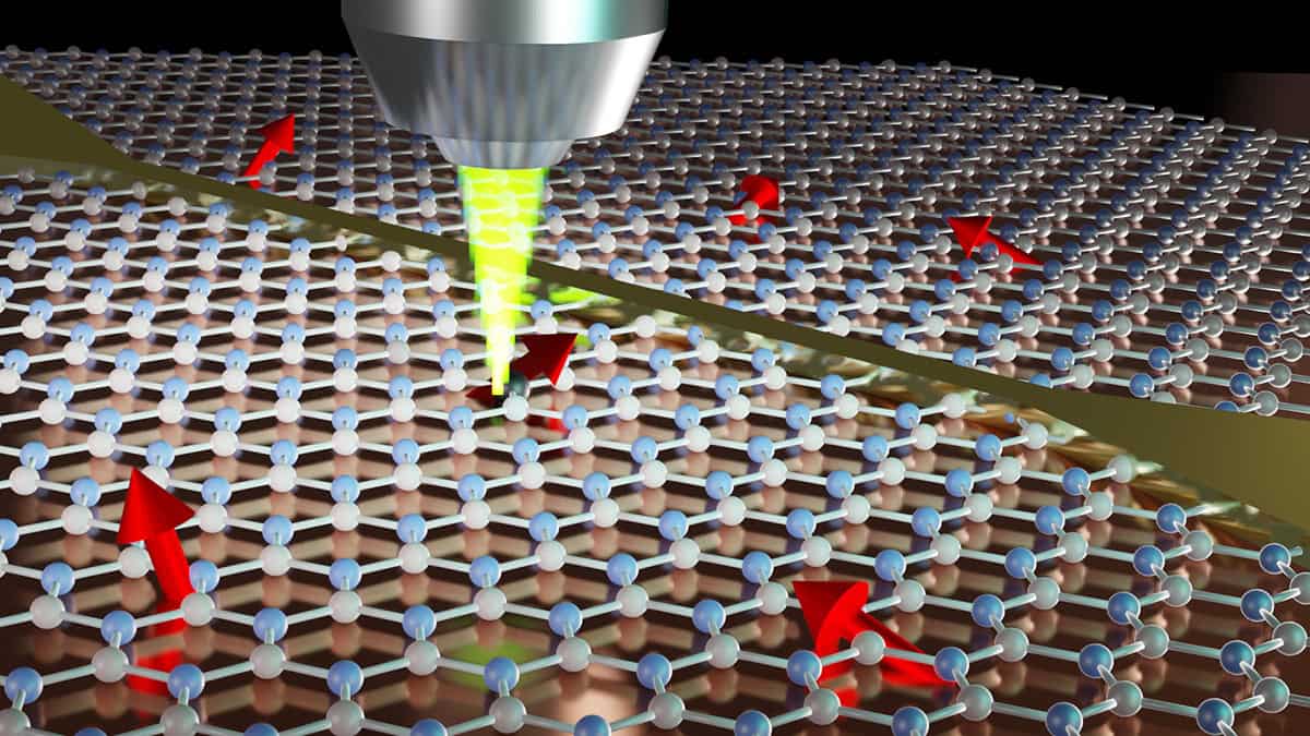
Handy tool Defects in the lattice structure of hexagonal boron nitride can be detected with photoluminescence, which is handy as such defects can be used under ambient conditions for applications in quantum technology. (Courtesy: Qiushi Gu)
The next thing will also be to control the growth of the hBN better and we’re working with collaborators on that. We want to create a defect exactly where we want it in the 2D material. This is a massive challenge but we’re hopeful that the 2D material will enable this.
Further work will also involve working with companies who are interested in this space, eventually moving towards implementing this material in a full device.
The quantum sector has been growing rapidly but what are the biggest challenges in commercializing the technology?
We are at a point now as a community where a lot has been demonstrated in laboratories and many of the existing challenges are about scaling. For quantum computation with solid-state spins, this means scaling to more and more qubits, while for optical networking, it’s about scaling to more and more nodes.
To achieve scalability, we need to interface different materials with each other and interface quantum systems with classical electronics and optical components
There are also challenges related to materials development. To achieve scalability, we need to interface different materials with each other and interface quantum systems with classical electronics and optical components. One part of achieving this that I’m particularly interested in is identifying new quantum systems in new materials that offer advantages or alternative possibilities alongside the existing ones.
We’re seeing that this is an exciting new direction in the field – to look at other material systems and explore these to build a broader material toolkit.
You’ve recently set up your own group in Manchester. What do you want its ethos to be?
The group is multidisciplinary and interdisciplinary and I think that’s important. We cover physics, chemistry, materials science and electronic engineering. Having a lot of different views in the room and scientific backgrounds encourages creativity, and it also contributes to scientific risk-taking. In some respects, the work on defects in hBN was risk-taking at the beginning because we didn’t know what we would find.
I’m also hoping to build a group where anyone from any background, nationality or minority is welcome. I think it’s important the group be broadly inclusive and representative of society. I’ll work hard to make sure it stays that way.
Researchers at Manchester University in the UK have used graphene to make a new electrically-controlled switching device that supports both memory and logic functions. The device, which exploits graphene’s ability to conduct protons as well as electrons, might also be used in applications that involve an electrode-electrolyte interface, such as reducing carbon dioxide to its component chemical species.
Graphene is a two-dimensional sheet of carbon atoms arranged in a honeycomb-like hexagonal lattice. One unique property of graphene is that electrons move freely through the plane of this sheet at almost ballistic speeds, making it a better conductor than metals. Another fascinating property is that when an electric field is applied between the top and the bottom of the sheet, protons from an adjacent polymer or electrolyte will flow through it in a perpendicular direction.
These flows of particles are not independent, however. Some of the protons bind to the electrons, and this binding process, known as hydrogenation, produces defects that scatter and slow the remaining unbound electrons. When the number of bound electrons reaches a threshold, the material turns into an insulator. The material’s conductivity can then be restored by applying an electric field in the plane of the graphene sheet, injecting more electrons into it.
Controlling the movement of the electrons and protons independently
Researchers led by Marcelo Lozada-Hidalgo have now exploited these proton and electron flows to perform logic and memory operations in a single device for the first time. The device consists of a micron-scale graphene layer sandwiched between proton-conducting electrolytes that are connected to gate electrodes on the top and bottom of the device. Additional electrodes placed at the device’s edges induce electrons to flow through the graphene sheet. This arrangement allows the researchers to simultaneously measure the graphene sheet’s in-plane electrical conductivity and the degree to which protons permeate it in the out-of-plane direction.
Proton and electron transport with independent control of field and charge density: a) Diagram of the experimental setup showing the top and bottom voltages and the direction of electron and proton flow. b) Map of in-plane electronic conductance, σe, as a function of electric field E and charge density n. The left and bottom axes show that these variables are controlled by the difference and sum of the top and bottom electron voltages, respectively). c) Map of proton transport current, I, as a function of E and n. (Courtesy: M Lozada-Hidalgo)
Crucially (and unexpectedly, Lozada-Hidalgo says), the two-gate set-up also gave the researchers independent control over proton transport and the electron-proton binding that determines whether graphene is a conductor or an insulator. “We can drive proton transport without hydrogenating graphene or hydrogenate graphene without driving proton transport, or both,” he tells Physics World.
The source of this independent control, he explains, is that both hydrogenation and proton transport depend on the electric field E and the charge density n of the graphene. Using a non-aqueous electrolyte allows both E and n to be extremely high, which effectively distorts the energy profile for these processes. And while E depends on the difference between the top and bottom gate voltages, n depends on their sum, making it possible to tune E and n independently simply by altering the voltages. “Such control is impossible otherwise and is so robust and reproducible that we can exploit it to perform proton-based logic-and-memory operations in graphene,” Lozada-Hidalgo says.
A very different computing platform
In the latest study, which is published in Nature, the researchers demonstrated this capability by using the graphene layer’s conducting or insulating status as a “memory” state. At the same time, they used the proton current to perform a logic operation called the exclusive operation (XOR) that outputs a “1” when the number of inputs with a value of 1 is odd, and a “0” otherwise. Hence, when the top and bottom electrode voltages differed, the XOR operation yielded a 1, and a strong proton current flowed – without changing the state of the memory.
The fact that both logic and memory operations occur in the same device is significant, Lozada-Hidalgo says, because these functions are usually performed by separate circuit elements that are physically isolated from each other within a computer. This can lead to long data-transfer times and high power consumption. “Our work could perhaps enable low-cost analogue computing structures that operate on protons,” he says. “At the very least, it is a very different computing platform that does not require silicon and can be implemented in very simple and potentially cheap devices.”
The fact that it uses protons, rather than electrons as in conventional circuits, could also make it possible to couple these devices with biological systems or electrochemical interfaces, he adds.
“A host of application areas”
While the Manchester researchers have so far only demonstrated these processes in graphene, they say that any 2D crystal could be studied in this way. “This represents a great opportunity for investigating electrode-electrolyte interfaces in a large group of materials and over a parameter space that is inaccessible in classical interfaces,” Lozada-Hidalgo says.
As well as memory-logic devices, he adds, the effect could be of interest in “a host of application areas”, including nanofluidics, catalysis, electrochemistry and surface science. “It’s a new technological capability in our discipline,” he says. “The electrochemical processes at play can be linked to the electronic properties of the 2D crystals because they can induce conductor-insulator phase transitions or strongly dope the materials and their heterostructures. We are looking into these possibilities now.”
It is a curious fact of climate science that clouds can both cool the Earth’s surface and keep it warm. This apparent paradox occurs because during the day, clouds reflect shortwave sunlight back into space thanks to the albedo effect, whereas at night they act like blankets, trapping longwave radiation close to the surface.
Researchers from Sun Yat-sen University in China and Leipzig University in Germany have now found that as the climate changes, cloud cover – especially in the lower atmosphere – decreases more during the day than at night. This asymmetry, they say, could contribute to a feedback spiral that makes planet warmer still.
“Our findings show that there is an even greater need to reduce greenhouse gases,” explains Johannes Quaas, the meteorologist who led this study, “because not only does cloud cover respond to warming, it also amplifies warming through this new effect.”
Daily variations
Other studies have previously shown that nighttime temperatures are increasing faster than daytime ones. The reason for this is not yet clear, however, as several feedback processes (including changes in cloud cover, atmospheric humidity, soil moisture and aerosol emissions) may be contributing to it.
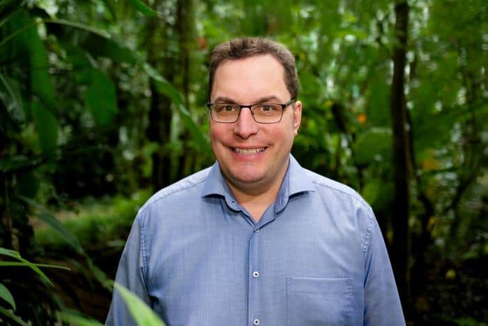
Clouds covered: Research leader Johannes Quaas. (Courtesy: Antje Gildemeister)
In their work, which they detail in Science Advances, Quaas and colleagues studied how daily variations in cloud cover affect climate. The diurnal asymmetry in cloud cover they identified could stem from several factors, but the main one is that rising concentrations of greenhouse gases have made the lowest layer of the atmosphere (known as the lower troposphere) more stable. “This enhanced stability is having a negative effect overall,” says Quaas. “Less clouds are forming during day (so reducing their sunlight-reflecting effect), but they are remaining more stable at night (so increasing their blanket effect, in relative terms).”
The researchers obtained their results by analysing satellite observations and data from the sixth phase of the Coupled Model Intercomparison Project (CMIP6), which incorporates both historical data collected between 1970 and 2014 and projections up to the year 2100. “We found some day-night differences and started to wonder whether there might be a systematic effect in a warming climate,” Quaas says.
The fact that these differences had not been studied before, he adds, may be due to the way climate researchers tend to analyse data. “When looking at global climate, one typically uses one time of day, or averages over time and analyses the geographical distribution,” Quaas explains. “Climate models for their output, and satellite observations, thus choose one time zone for the entire globe – typically UTC (Greenwich time). It took us the extra step to convert this to local time to see our result. Not a very elaborate idea, admittedly, but one that turned out to be revealing.”
While the asymmetry effect is not huge, it is systematic, he tells Physics World. “Effects such as those on solar energy are not going to be overwhelming, but are an important supplement to global warming,” he says.
The researchers now want to explore other factors – beyond the changes in atmospheric stability that they have identified – that may also be driving changes to cloud cover. “One such reason could be deforestation, for example,” Quaas suggests.
A theoretical study has confirmed that a particle observed at CERN’s LHCb experiment in 2022 is indeed a tetraquark – supporting earlier hypotheses that were based on the analysis of its observed decay products. Tetraquarks comprise four quarks and do not fit into the conventional classification of hadrons, which defines only mesons (quark and an antiquark) and baryons (three quarks). Tetraquarks are of great interest to particle physicists because their exotic nature provides opportunities to deepen our understanding of the intricate physics of the strong interactions that bind quarks together in hadrons.
“X(3960) is a new hadron discovered at the Large Hadron Collider (LHC),” Bing-Dong Wan of Liaoning Normal University and Hangzhou Institute for Advanced Study, and the author of the study, tells Physics World. “Since 2003, many new hadrons have been discovered in experiments, and some of them appear to be tetraquarks, while only a few can be confirmed as such.”
Named for its mass of 3.96 GeV – about four times that of a proton – X(3960) stands out, even amongst exotic hadrons. Its decay into D mesons containing heavy charm quarks implies that X(3960) should contain charm quarks. The details of the interaction of charm quarks with other strongly interacting particles is rather poorly understood, making X(3960) interesting to study. Additionally, by the standards of unstable strongly interacting particles, X(3960) has a long lifetime – around 10-23 s – indicating unique underlying quark dynamics.
These intriguing properties of X(3960) led Wan to investigate its structure theoretically to determine if it is a tetraquark or not. In a recent paper in Nuclear Physics B, he describes how he used Shifman-Vainshtein-Zakharov sum rules in this calculations. This approach examines strongly interacting particles by relating their properties to those of their constituent quarks and the gluons that bind them together. The dynamics of these constituents can be accurately described by the fundamental theory of strong interactions known as quantum chromodynamics (QCD).
Wan assumed that the X(3960) is composed of a strange quark, a charm quark and their antiparticles. Using the sum rules, he derived its mass and the lifetime to compare these parameters with the observed values.
Mathematical machinery
Using the mathematical machinery of QCD and extensive numerical simulations, he found that the mass of the tetraquark he formulated is 3.98 ± 0.06 GeV. This is a close match to the measured mass of X(3960) at 3.956±0,005 GeV. This confirms that X(3960) comprises a strange quark, a charm quark and their antiparticles. Furthermore, Wan was able to compute the lifetime of his model particle to be 1.389±0.889×10⁻²³ s, which aligns well with the observed value of (1.53−0.26+0.41)×10−23 s, further validating his identification.
While Wan’s work strongly supports the hypothesis that X(3960) is a charm–strange tetraquark, he acknowledges that it is not conclusive proof. In the subatomic world, particles can transform into others and the match of the quark composition of the tetraquark he studied and the decay products of X(3960) is not enough, Indeed, in principle, X(3960) can be even better described by some other quark composition.
“There are many possible structures for tetraquarks, and my work finds that one possible structure can explain the properties of X(3960),” says Wan. “But some other researchers may be able to explain the properties of X(3960) using different quark structures.”
To further validate his approach, Wan applied the sum rule technique to a particle similar to X(3960), called X(4140), previously discovered at the Tevatron collider. His calculations yielded mass and lifetime values very close to the measured ones, further confirming his method’s accuracy.
However, to definitively determine the structure of X(3960), further theoretical and experimental studies are needed. Analysing a larger number of decay events will help reduce measurement errors. On the theoretical side, using the sum rules or other QCD techniques to more accurately analyse these parameters will help reduce computational uncertainties.
“Studying new hadrons may greatly enrich the hadron family and our knowledge of the nature of strong interactions,” Wan concludes. “It is highly expected that we are now at the dawn of enormous discoveries of novel hadronic structures, implying a renaissance in hadron physics.”
The physicist Rosemary Fowler has had to wait three quarters of a century to be honoured for her role in discovering a subatomic particle.
Fowler was doing a PhD at the University of Bristol in 1948 under the supervision of physicist Cecil Powell when she stumbled upon the particle.
The then 22-year-old physicist spotted unusual particle tracks in photographic emulsions that had been exposed to cosmic rays at high altitude in Switzerland.
She discovered a particle that decayed into three pions and labelled the track ‘k’, with the particle now known as the K-meson or “kaon”.
“I knew at once that it was new and would be very important,” Fowler noted. “We were seeing things that hadn’t been seen before – that’s what research in particle physics was. It was very exciting.”
The results were published in two papers in Nature with Fowler (née Brown) as first author. She then decided to leave university and married fellow Bristol physicist Peter Fowler – the grandson of Ernest Rutherford – in 1949. They had three children, all of whom went on to study science. Peter died in 1996.
This week Fowler, who is 98, was finally honoured for her work. She received an honorary doctorate from Bristol University in a private graduation ceremony held near her Cambridge home.
Fowler said she felt “very honoured” by the doctorate, but added humbly that she hadn’t “done anything since to deserve special respect”.
As electromagnetic waves travel, they collect information about their environment. This property is widely exploited in a host of applications that rely on waves being deflected, scattered or reflected off their surroundings, but it comes with a challenge: how can we extract as much of this information as possible?
Researchers in Austria and France have now developed a new mathematical formalism that may help answer this question. The information the wave carries about its environment is known as Fisher information, and the new formalism makes it possible to visualize how waves collect this information from objects they interact with as they travel.
“The basic idea is quite simple: you send a wave at an object and the part of the wave that is scattered back from the object is measured by a detector,” explains theoretical physicist and study lead Stefan Rotter from TU Wien. “The data can then be used to learn something about the object – for example, its precise position, speed or size.”
Continuity effects
Rotter and colleagues found that a wave’s Fisher information matches a “continuity equation”, meaning that the information contained in the wave is preserved as it propagates, and obeys laws not dissimilar to the laws of energy conservation. This continuity equation allowed the researchers to calculate precisely where in the wave the information is actually located. They also discovered that different types of information on the properties of an object (such as its position, speed and size) are carried in different portions of the wave and that this information depends, with high precision, on how strongly the wave is affected by specific object properties.
“For example, if we want to measure whether an object is a little further to the left or a little further to the right, then the Fisher information is carried precisely by the part of the wave that comes into contact with the right and left edges of the object,” says TU Wien team memberJakob Hüpfl. “This information then spreads out, and the more of this information reaches the detector, the more precisely the position of the object can be read from it.”
Experimental tests in microwaves
The researchers tested their theory experimentally with help from collaborators in Ulrich Kuhl’s group at the University of Côte d’Azur in Nice. “We suggested that Felix Russo, a new masters student in our group, would be interested in carrying out the experimental part of the work and Kuhl agreed to host and supervise him,” says Rotter.
Russo began by sending microwaves through a structure made up of several randomly-positioned Teflon objects and a single metallic rectangle. The aim of the experiment was to determine the position of this rectangle by analysing data received at a detector on the other side of the structure.
“By precisely measuring the microwave field, it was possible to show exactly how the information about the horizontal and vertical position of the rectangle spreads: it emanates from the respective edges of the rectangle and then moves along with the wave – without any information being lost,” Russo says.
Applications in different fields
Rotter says the team’s formalism opens up a new way of thinking about how waves retrieve information from their environment. “Since this is such a widely used concept – ranging from seismology to biomedical imaging and from radar technology to quantum sensing – I expect our results to be useful in quite a broad range of different fields,” he tells Physics World.
The Vienna-Nice researchers are now working on extending their theory to multi-parameter sensing protocols and applying it to specific experimental settings. “Our goal is to demonstrate the advantages that can be gained in terms of designing an experiment and in improving the resulting measurement precision by using our technique,” Rotter says.