At a Glance: Phononic crystals
- When a wave passes through a periodic structure, interference leads to the formation of “band gaps” that prevent waves with certain frequencies travelling through the structure
- Band gaps have been observed for electron waves in semiconductors, electromagnetic waves in photonic crystals and sound waves in phononic crystals
- The periodic variation in the density and/or speed of sound that is needed to make a phononic crystal can be achieved by making “air holes” in an otherwise solid structure
- The phenomenon of “negative refraction” – which can be exploited to make superlenses that can beat the diffraction limit – has been observed with phononic crystals
- Controlling the dispersion relation for phonons both inside and outside the band gap could lead to breakthroughs in both fundamental research and applications
It is fascinating to think of the abstract beauty of crystals, with countless atoms occupying precise positions on a lattice and giving rise to perfect order and high levels of symmetry. Indeed, we need look no further than the brilliant appearance and extraordinary properties of many precious gems to witness the consequences of these precise atomic arrangements.
This picture of crystals is very appealing, but it is not strictly correct. Even in an ideal crystal that is free from defects, the atoms are never static – they are always moving randomly around their equilibrium positions. Scientists have long assumed that it is impossible to control this random thermal motion. However, a novel class of artificially structured materials known as “phononic crystals” might make such control possible.
Phononic crystals make use of the fundamental properties of waves, such as scattering and interference, to create “band gaps” – ranges of wavelength or frequency within which waves cannot propagate through the structure. This phenomenon is well known in physics: the electrons in a semiconductor can only occupy certain energy bands, while photonic crystals only allow light in certain frequency ranges to travel through them.
The band gap in a photonic crystal is caused by a periodic variation in the refractive index of an artificially structured material. In a phononic crystal the density and/or elastic constants of the structure change periodically. This changes the speed of sound in the crystal, which, in turn, leads to the formation of a phononic band gap.
But why mention waves at all when talking about random atomic motions? The reason is that the atoms in a solid cannot move independently of each other because they are connected by chemical bonds. When an atom is displaced from its equilibrium position, it exerts a force on its neighbours, which causes them to move. These atoms then cause their neighbours to move, and the end result is the creation of a “phonon” – a special wave of lattice distortion that propagates through the solid.
Where do band gaps come from?
Acoustic waves differ from light waves in several ways. Acoustic waves are mechanical, which means that they cannot travel through a vacuum, whereas light waves are electromagnetic and can travel through a vacuum. In general, mechanical waves passing through a gas or a liquid are known as acoustic waves, while those passing through a solid are called elastic waves.
There are other important differences between mechanical and electromagnetic waves. Whereas a light wave can have two independent polarizations, an elastic wave in a homogeneous solid has three independent polarizations: two of these are transverse (shear waves) and one is longitudinal (a compression wave). However, since shear waves are not supported in liquids and gases, an acoustic wave has just one longitudinal polarization.
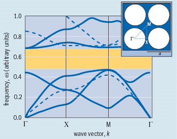
The propagation of mechanical waves in a medium is usually described by a dispersion relation that relates the frequency, w, and wave vector, k, of the propagating wave. The dispersion relation for waves travelling in a homogeneous medium is very simple: ω =c • k, where c is the velocity of sound in the medium. However, the dispersion relations for materials that are not homogeneous – such as phononic crystals (figure 1) – are more complicated.
But why are certain waves not allowed to propagate in phononic crystals? To get an intuitive understanding of how band gaps form, consider a 1D crystal composed of alternating layers of two different materials. At every interface an incoming wave transfers part of its energy into secondary, reflected waves, which then interfere with each other.
If this interference is constructive, all the energy of the original wave is reflected back and the wave cannot propagate through the crystal. On the other hand, if the interference is destructive, then all energy of the original wave is transmitted through the crystal. Therefore, constructive interference of the secondary waves results in the creation of a band gap, while destructive interference leads to the formation of propagation bands.
The condition for constructive interference is simply that the path differences between the interfering waves must be equal to an integer multiple of their wavelength, λ. Since the path difference is determined by the lattice parameter of the crystal, a, it is easy to see that constructive interference occurs when the lattice parameter is comparable to the wavelength. And since frequency is inversely proportional to wavelength, the frequency at the centre of the band gap, wg, is also inversely proportional to the lattice parameter: ωg ∼ 1⁄λ ∼ 1⁄a. As a result, we can create a band gap at any frequency or wavelength we choose by simply changing the size of the unit cell. The width of the band gap is directly related to the ratio of the densities and sound velocities in the different layers: the larger the ratio, the wider the gap.
Moreover, the position and width of the band gap depend on the direction of the waves because the path difference depends on the angle of incidence. Some phononic crystals form band gaps for waves propagating in any direction – these are known as absolute or complete band gaps. Other materials possess partial band gaps that only stop waves travelling in certain directions. It is easy to see that a 1D crystal does not have an absolute band gap because its mechanical properties only vary in one direction: waves travelling at right angles to this direction will not be reflected, so there will not be a band gap in this direction.
Symmetry and phononic band gaps
How do we design a phononic crystal to have a complete band gap? It is clear from our 1D example that the density and sound velocity need to vary in all three directions of space. However, very few 3D periodic structures will form a complete phononic band gap. In fact, it is still quite difficult to determine the structures with large absolute band gaps. For electromagnetic waves, which only have two independent (transverse) polarizations, sinusoidal modulations of the dielectric constant along certain directions create photonic crystals with absolute gaps for three different, highly symmetric lattices: simple cubic, body-centred cubic and face-centred cubic. The diamond structure, which is face-centred cubic, possesses the champion photonic band gap, i.e. the largest band gap for a given dielectric constant.
Mechanical waves can have both longitudinal and transverse components in a solid, although only longitudinal waves are allowed in fluids. As a result, if we want to create a complete phononic band gap, we must design structures that have band gaps for both longitudinal and transverse waves in the same frequency region. This could be harder than designing structures for photonic crystals because electromagnetic waves only have transverse modes.
The search for structures with complete phononic band gaps began in 1992 with theoretical work by Michael Sigalas and Eleftherios Economou while they were both at Iowa State University in the US. They showed that structures that consist of a periodic 3D lattice of identical high-density spheres placed within a low-density host material gave rise to phononic band gaps. These structures can either be solid-solid or liquid-liquid.
Despite the fact that elastic waves propagate at two different speeds in solids while acoustic waves propagate at a single speed in fluids, Sigalas and Economou predicted that complete phononic band gaps should exist in solid-fluid structures, as well as solid-solid and fluid-fluid structures. A few months later they showed that an infinite 2D array of high-density parallel cylinders embedded in a low-density host material should also possess a complete band gap in two dimensions. Unaware of this work, Manvir Kushwaha of the Universidad Autónoma de Puebla and co-workers reported the existence of phononic band gaps for polarized elastic waves in 2D elastic systems in 1993.
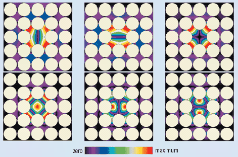
The existence of structures with complete phononic band gaps has obvious applications. For instance, a phononic crystal will reflect incoming sound waves with frequencies within the gap and can therefore be used as an acoustic isolator. Moreover, the introduction of defects within the structure allows sound waves with frequencies in the band gap to be trapped near a point-like defect (figure 2), or guided along linear defects.
Phononic crystals and sound
Sound manipulation is perhaps the most obvious application of phononic crystals. Sound is immensely valuable in our daily lives for communication, information transfer or simply for its aesthetic value as exhibited in music and rhythms. For human hearing, sound is basically made up of acoustic waves with frequencies roughly between 20 Hz and 20 kHz, or wavelengths ranging from metres to several tens of centimetres. Therefore, if we assemble periodic structures with lattice constants in this range, we can expect them to inhibit sound and act as sonic mirrors.
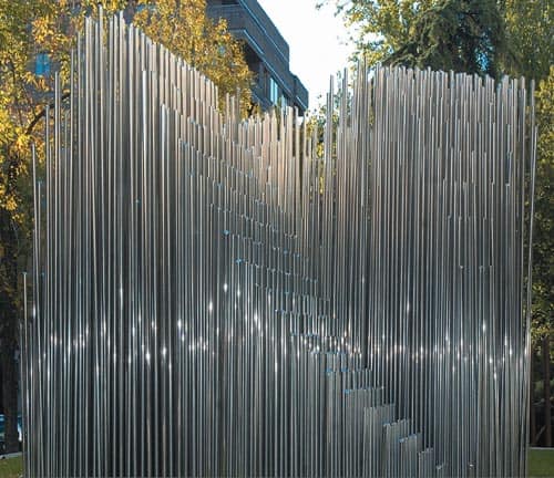
A great illustration of the sonic properties of a periodic structure was provided by Francisco Meseguer and co-workers at the Materials Science Institute of Madrid in 1995 when they studied the acoustic characteristics of a kinematic sculpture by Eusebio Sempere (figure 3). This minimalist sculpture consists of a periodic square array of hollow steel cylinders.
In addition to being visually appealing, Meseguer and co-workers recognized that the sculpture should also possess a sonic band gap, so they measured the acoustic transmission of the sculpture as a function of frequency and direction. They found that sound travelling perpendicular to the axes of the cylinders was strongly attenuated at a frequency of 1670 Hz – a result that provided the first experimental evidence for the existence of phononic band gaps in periodic structures (Nature 378 241).
Unfortunately, a structure needs to be several metres wide to create a phononic band gap in the sonic regime. While this might not be a problem for architectural acoustics, it is impractical for many other devices such as headphones and speakers. However, if we move to the ultrasonic regime, the relevant wavelengths are much shorter, so the phononic crystals are also much smaller (from centimetres down to fractions of millimetres). This smaller length scale – combined with negative refraction, superlenses and other advances – could lead to a wide range of applications for phononic crystals.
Ultrasound, negative refraction and superlenses
One of the hottest topics in optics over the past five years has been the possibility of making “superlenses” with materials that have a negative refractive index. And just as photonic band gaps were followed by phononic band gaps, recent progress in making superlenses for electromagnetic waves has prompted efforts to make superlenses for acoustic waves.
In general it is not possible for a conventional lens to produce an image that contains details that are finer than the wavelength of the light being focused. However, superlenses made of “negative index” materials can overcome this diffraction limit. Moreover, these superlenses do not even have to be shaped like traditional lenses – a flat, thin slab of negative-index material can act as a superlens, which means that they should, in theory, be much easier to fabricate than traditional lenses.
In optics the challenge has been to make materials that have a negative refractive index at the appropriate wavelength (see “Superlens breaks optical barrier” Physics World August pp23-24). Recent research suggests that it might be possible to make acoustic superlenses with phononic crystals.
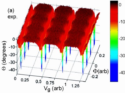
The speed of light or sound in a medium depends on the refractive index of that medium. And when light or sound travels from one medium into another with a different refractive index, both its speed and direction change. This is refraction. Most traditional materials exhibit positive refraction, but some specially designed materials can exhibit negative refraction (figure 4).
Negative refraction in phononic crystals is possible due to multiple scattering of sound waves at the solid-air interfaces. To get an intuitive understanding of negative refraction consider a sound wave moving through a homogeneous medium that strikes a phononic crystal at an angle. We can think of the sound wave as having two components: one that travels parallel to the surface, and one that moves at right angles to it. Negative refraction will occur if the direction of the parallel component is reversed while that of the normal wave does not change. This is actually possible if the parallel component is reflected by the phononic crystal while the normal wave is allowed to propagate.
In 2004 Xiandong Zhang of Beijing Normal University and Zhengyou Liu of Wuhan University, both in China, predicted that negative refraction would occur in 2D hexagonal “fluid-fluid” crystals consisting of water cylinders in a mercury matrix. They used a detailed analysis of a phononic band diagram to derive conditions for all-angle negative refraction of acoustic waves, and simulated the propagation of a wave through a flat slab of negative-refraction material.
Meanwhile, Jian Zi and co-workers at Fudan University, also in China, demonstrated experimentally a superlens for liquid surface waves for the first time in 2004 (figure 4). The development of superlenses for acoustic waves would be a major breakthrough for a variety of ultrasound techniques.
Hypersound and thermal management
Wavelengths in the hypersonic regime are even shorter than those used for ultrasound. Indeed, hypersonic wavelengths are less than 10 μm, which corresponds to frequencies higher than 100 MHz. However, the behaviour of hypersonic phonons is crucial for many physical phenomena in materials. For example, the interaction between electrons and high-frequency phonons determines the efficiency of spontaneous light emission in silicon and other semiconductor materials that have an “indirect” electronic band gap. Greater control over the phonons in silicon could therefore lead to highly efficient silicon-based light-emitting devices. Making such devices is a major goal for the optoelectronics industry.
Hypersonic phononic crystals could also have a large impact in thermal management. Thermal energy in solids is transported primarily by electrons and phonons. The electronic contribution is important for materials with a large number of free carriers, such as metals. On the other hand, the thermal conductivity of dielectric materials and many semiconductors is determined mainly by the phonons. The presence of a phononic band gap would reduce the flow of phonons and therefore the thermal conductivity of a solid.
This could prove very useful for thermoelectric devices that directly convert thermal energy into electricity. The figure of merit for a thermoelectric device, which is known as ZT, scales as ZT ∼ σ ⁄(ke + kph), where σ is the electrical conductivity, and ke and kph are the electronic and phononic heat conductivities, respectively. If we reduce the electronic heat conductivity, ke, we will also reduce the electrical conductivity, σ, which means that ZT will not increase. However, by using a phononic band gap to reduce the phononic heat conductivity, kph, it could be possible to greatly improve the performance of devices such as Peltier thermoelectric coolers, thermocouples and thermoelectric energy generators.
However, it is not easy to design and fabricate hypersonic crystals. In contrast to sonic and ultrasonic crystals, which are macroscopic and can be readily made using standard manufacturing techniques, hypersonic crystals require 3D periodic patterns to be created at the submicron and nanometre scale. A variety of techniques are being explored for the fabrication of such structures. For example, some researchers are trying to build hypersonic crystals from alternating layers of two materials using lithography-based techniques from the semiconductor industry. Others use two-photon lithography to pattern the inside of photosensitive polymers with lasers. Some groups are also investigating self-assembly techniques.
Each of these methods has a variety of advantages and drawbacks. Recently another approach – holographic interference lithography – has received much attention. Since light is inherently periodic, the overlap of multiple beams of light can result in interesting periodic patterns. For example, when two laser beams are brought together, they form a 1D periodic intensity pattern, while the interference of three beams results in 2D patterns and so on.
If the laser beams overlap inside a photosensitive material, it is possible to turn the light intensity pattern of the light into a solid structure. At the Massachusetts Institute of Technology (MIT) we have recently been able to fabricate various 2D and 3D periodic structures using interference lithography and then, working with George Fytas at the Max Planck Institute for Polymer Research in Mainz, Germany, directly measure their phononic dispersion relation using Brillouin light scattering. Previously, Maya Campbell, Andrew Turberfield and co-workers at Oxford University had used interference lithography to make photonic crystals.
“Blind” and “deaf” materials
Since the same basic ideas underpin both phononic and photonic band-gap materials, it seems obvious to explore the possibility of making materials that exhibit both types of band gap. Indeed, at MIT two of the present authors (MM and ELT) have recently designed a crystal that is “blind” to electromagnetic waves with wavelengths of about several hundred nanometres and “deaf” to sound at similar wavelengths within the crystal. These crystals consist of a square or triangular 2D array of air holes in silicon. In addition to having complete band gaps for both light and elastic waves, we have found that they can also simultaneously trap sound and light at defects.
The ability to make structures with both types of band gap could lead to breakthroughs in the field of acousto-optics. In 1997, for example, Harold de Wijn and co-workers at the University of Utrecht in the Netherlands suggested that it might be possible to use these structures to generate intense sources of coherent monochromatic phonons, which could be known as “phonon lasers”. Other applications could include optical cooling in solids and optical frequency-conversion devices.
In 2002 Alex Fanstein and co-workers at the Centro Atómico Bariloche in Argentina and the LPN-CNRS laboratory at Marcoussis in France measured photon-phonon scattering in 1D periodic structures that contained both photonic and phononic band gaps. Since all the layers in the phononic structure were only several nanometres thick, they did not get in the way of the light. Fanstein and co-workers showed that such double localization of photons and phonons increases the efficiency of photon-phonon scattering by five orders of magnitude compared with the values for similar 1D structures with photonic cavities only.
The field of phononic crystals is only about 10 years old and many important questions are just being raised. The search for the best phononic structure is ongoing, but even the very definition of the “best phononic structure” still needs to be clarified. What goes on outside the band gap is often just as important in phononic applications.
Negative refraction, for instance, is made possible by the unusual properties of the dispersion relation in the propagation band. And to get light out of silicon with the help of phonons it is necessary to increase rather than decrease the phononic density of states. We must therefore think in terms of engineering the dispersion relation for phonons, rather than simply making the band gap as large as possible.
Phononic crystals will provide researchers in acoustics and ultrasonics with new components that offer the same level of control over sound that mirrors and lenses provide over light. But hypersonic phononic crystals can also be used for fundamental science. They could, for example, be used to explore changes to the statistical distribution of random phonons under equilibrium and non-equilibrium conditions, or to study how phononic band gaps affect the thermal properties of materials.
It is difficult to predict how the field of phononic crystals will develop in the future, but one thing is clear: we will hear a lot more about these materials in every sense of the word.
More about: Phononic crystals
G Chen et al. 2004 Engineering nanoscale phonon and photon transport for direct energy conversion Superlattices and Microstructures 35 161
T Gorishnyy et al. 2005 Hypersonic phononic crystals Phys. Rev. Lett. 94 115501
J Sánchez-Dehesa 2004 Phononic crystals bring sound to a focus Physics World September p23
M M Sigalas and E N Economou 1993 Band structure of elastic waves in two-dimensional systems Solid State Commun. 86 141
M Trigo et al. 2002 Confinement of acoustical vibrations in a semiconductor planar phonon cavity Phys. Rev. Lett. 89 227402
X Zhang and Z Liu 2004 Negative refraction of acoustic waves in two-dimensional phononic crystals App. Phys. Lett. 85 341