Purity pays off for nanotubes

The features in conventional microelectronic circuits are getting smaller and smaller and will soon reach the limit imposed by the fundamental properties of silicon. Scientists hope that carbon nanotubes – which are essentially rolled up sheets of graphite, just nanometres in diameter, with excellent electronic and mechanical properties – might one day be used to replace silicon in electronic circuits.

Large quantities of single-walled nanotubes can be produced by the high-pressure decomposition of carbon monoxide (HiPCO) method. However, nanotubes grown by this technique usually contain large amounts of carbon-based impurities that degrade the properties of nanotube devices.

The purification method developed by Alan Johnson and colleagues at the University of Pennsylvania begins by heating nanotubes produced by the HiPCO method in wet air in the presence of hydrogen peroxide, followed by a gentle acid treatment. Next, magnetic fields are used to separate the nanotubes from the impurities. The semiconductor chips are then dipped into a solution containing the nanotubes to create circuits. “Ultimately we can make it so the nanotubes only stick where we want them to in order to form a circuit,” explains lead author Danvers Johnston.

The UPenn team has already made field-effect transistors from the purified nanotubes and shown that they have superior properties compared with devices made from non-purified HiPCO material. Moreover, they have shown that they can determine the energy gap of individual semiconducting nanotubes by measuring the current in their circuits and varying the temperature and gate voltage.
Solar system gets bigger

Mike Brown of the California Institute of Technology, Chad Trujillo of the Gemini Observatory in Hawaii and David Rabinowitz of Yale University discovered 2003 UB313 with the Samuel Oschin telescope at the Palomar Observatory in California. They first photographed the new planet in October 2003 but it was so far away that they did not actually realize it might be a planet until they reanalysed their data in January this year.

2003 UB313 lies in a vast band of small, icy bodies beyond Neptune called the Kuiper belt. The new planet seems to be typical of Kuiper-belt objects but is much bigger — between about 2300 and 3200 km wide. Pluto is 2390 km across. “Its sheer size in relation to the nine known planets means it can only be classified as a planet itself,” says Brown.

Brown and colleagues have already obtained near-infrared spectra of the new planet with the Gemini North Telescope, which show signatures of methane ice very similar to the spectrum of Pluto. The presence of methane ice indicates a pristine surface that has not been significantly heated since the solar system was formed about 4.5 billion years ago. The discovery suggests that other “transneptunian” objects may be hiding undiscovered in the far reaches of the Solar System. Last year Brown and colleagues discovered an object called “Sedna”, which was previously the most distant object in the Solar System.

Meanwhile, astronomers at the Sierra Nevada Observatory in Spain have discovered a second large Kuiper-belt object called “2003 EL61”. This object is about two-thirds the size of Pluto and is about 51 astronomical units (AU) away from the Sun, where 1 AU is the average distance between the Earth and the Sun. Pluto, by comparison, is about 39 AU from the Sun.

Quantum boost for optical clocks

The “ticks” in an atomic clock are defined by oscillations between two energy states in an atom. Existing atomic clocks rely on microwave transitions in caesium atoms, but devices based on much faster optical transitions would be even more accurate. Such clocks could lead to the second being redefined and could also be used to check if the fundamental physical constants are truly constant.

An aluminium ion is a good candidate for making an optical clock because it has a very narrow transition between two of its energy states. However, it is difficult to study because it cannot be cooled or measured with existing laser techniques. David Wineland and colleagues at the National Institute of Standards and Technology (NIST) in Boulder, Colorado, have now overcome this problem by coupling the aluminium ion to a beryllium ion, which is easy to cool and measure. The use of extremely cold ions leads to more accurate measurements because it reduces the Doppler shifts that would otherwise broaden the transition line being observed.

The NIST team began by trapping the two ions in an electromagnetic Paul trap and then used a laser to create a quantum superposition of the ground and excited state of the aluminium ion. Both ions were then cooled to the motional ground state of the trap. Next another laser was applied to transfer the internal state of the aluminium into a superposition of the motional states of the two ions: roughly speaking, the two states in the superposition were both ions at rest and both ions moving together. Finally, they applied a laser pulse that transferred this superposition to a superposition of internal states in the beryllium ion, which they can probe with well establish laser spectroscopy techniques.

“In this way, we can detect the state of the beryllium ion, which gives us the same answer as if we had been able to detect directly on the aluminium ion,” says lead author Piet Schmidt, who is now at the University of Innsbruck in Austria. “This opens the door for spectroscopy of many more atomic species with interesting spectroscopic properties.” The technique could also be used to investigate the possibility of using boron, helium and other atoms as optical clocks.

Geoneutrinos make their debut

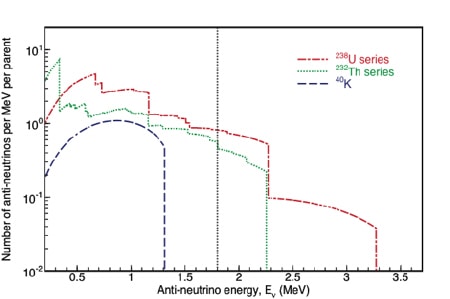
Neutrinos are very difficult to detect because they are electrically neutral and only interact weakly with matter, which means that they can pass through thousands of kilometres of matter without being absorbed. The Kamioka Liquid scintillator antineutrino detector (KamLAND) comprises a balloon with a diameter of 13 metres contains about 1000 tonnes of liquid scintillator. It identifies antineutrinos by counting the number of telltale flashes of light that are produced when antineutrinos occasionally collide with protons in the liquid to produce a positron and a neutron.

The amount of light produced by the positron allows the energy of the neutrino to be determined, which enables the KamLAND team to distinguish between neutrinos from the decay of uranium and thorium and background neutrinos. Using this method, the experiment detects about one geoneutrino per month. The background sources include neutrinos produced by nuclear reactors, which have been used in other experiments to explore the fundamental properties of neutrinos.

The KamLAND results have already been used to place an upper limit on the heat generated by uranium and thorium inside the Earth. “Unlike previous estimates, which are based on indirect samples from meteorites, this is based on a direct measurement of the neutrinos produced by the decay of these isotopes,” team member Nikolai Tolich told PhysicsWeb. “The heat generated by uranium and thorium decay is the driving force for mantle convection, and hence plate tectonics and earthquakes. This result and future measurements using the same technique will provide useful inputs to Earth convection models.”

“We now have a diagnostic tool for the Earth’s interior in our hands,” added KamLAND spokesman Atsuto Suzuki. “For the first time we can say that neutrinos have a practical interest in other fields of science.”

Surfaces have built-in “fingerprints”

Russell Cowburn and co-workers at Imperial College London, Durham University and the University of Sheffield used a phenomenon called “laser speckle” to examine the structure of different surfaces. This technique is already routinely used to measure surface roughness in metal and paper and for visualizing blood in vivo. They scanned a focused laser beam over a sheet of white paper and used photodetectors to record the intensity of the light reflected from four different angles.

The physicists then quantified how much random fluctuations on the paper differed from the mean value (called the zero positional shift) and converted these values into 1s and 0s to obtain the fingerprint code. They obtained different codes for different sheets from the same pack (see figure), and achieved similar results for plastic credit and identity cards and cardboard packaging. Moreover, a sheet of paper could be identified even after it had been screwed up into a ball, submerged in water, baked at 180°C, scribbled on with ballpoint and black marker pens, and scrubbed with abrasives.

“Our findings open the way to a new and much simpler approach to authentication and tracking,” says Cowburn. “This is a system so secure that not even the inventors would be able to crack it since there is no known manufacturing process for copying surface imperfections at the necessary level of precision.”

The probability of two pieces of paper sharing the same fingerprint is less than 1 in 1027 and for smoother surfaces, such as plastic cards and cardboard, it is 1 in 1020 says the team. Furthermore, each fingerprint only takes up between 200 and 500 bytes of storage space in a database.

“The beauty of this system is that there is no need to modify the item being protected in any way with tags, chips or inks — it’s as if documents and packaging have their own unique DNA,” adds Cowburn. “This makes protection covert, low-cost, simple to integrate into the manufacturing process and immune to attacks against the security feature itself.”

Electric fields move water droplets

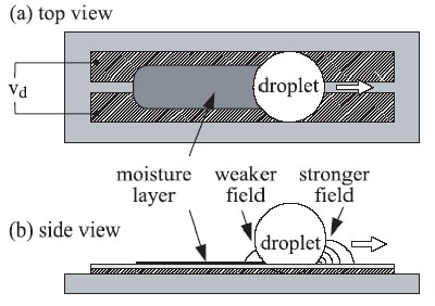
The Japanese team began by making a pair of parallel-strip electrodes on a glass substrate that had been covered by a thin electrically insulating hydrophobic layer and then placing a water droplet on the surface (figure 1). The droplet, which had a volume of between about 1 nanolitre and 1 microlitre, adopted an almost spherical shape due to a combination of surface tension and wetting effects.

To their surprise, the team found that the droplet began moving at speeds of up to 10 centimetres per second when a voltage was applied across the electrodes (figure 2). The initial direction of motion was unpredictable and the droplet continued to move until it reached the edge of the device or the voltage was switched off. Moreover, when the electrodes were made into the shape of a racetrack, the droplet kept travelling around the track (figure 3).

This motion came as a surprise because the electrodes used in the experiment create a uniform electric field along their length, so there is no energy gradient to move the droplets. According to Gunji and Washizu, the motion is “self-propelling” (figure 4). “The droplet leaves behind a moisture layer on the substrate surface, which shields the trailing edge of the droplet from the electric field,” says Washizu. “This produces an imbalance in the electrostatic force exerted on the droplet, which, in turn, provides the driving force for the droplet to move.”

It might be possible to use the new effect to automate chemistry experiments. “Many chemistry experiments are labour-intensive and are performed by mixing chemicals in test-tubes,” says Washizu. “If small liquid droplets could be transported across a substrate then chemical reactions could, in principle, be induced in small volumes by simply colliding the droplets together and mixing their contents.”

Atomic crystals go 2D

Geim and colleagues first made 2D crystals last year by peeling layers of graphene — 2D sheets of carbon atoms — from the surface of a thick crystal of graphite. They then used optical, electron-beam and atomic-force microscopy to separate out the thinnest films, which were just one carbon atom thick. The UK-Russia team also used standard lithography techniques to process the films, which have useful electronic properties, to make field-effect transistors (FETs).

Now, however, the group has found that the technique can be used on almost all layered materials, in which individual atomic planes are bound together only weakly. They have, for example, made 2D crystals from boron nitride, several dichalcogenides and various complex oxides. Furthermore, Geim and colleagues found the crystals were stable for several weeks at room temperature and that most of them kept their structural and electronic properties.

“For years there was a discussion if 2D materials should exist or not,” says lead author Kostya Novoselov. “Now that we have proved that 2D crystals exist and that they are stable, we can study their electronic, optical and mechanical properties. And it’s a whole new class of materials, which include metals, insulators, semiconductors and probably magnetic materials.” The discovery will also allow theoretical models of 2D materials to be tested. “These are very exciting materials to work with,” adds Novoselov. “We can study almost any property of matter in 2D.”

Applications include field-effect transistors, highly sensitive gas sensors, electromechanical devices and translational motors.

Timing electrons

Dynamical processes are usually studied by exciting a system with a pulsed pump laser operating at visible wavelengths and tracking how the system evolves using a second, probe pulse. However, these pulses usually last several femotseconds long and so cannot be used to study processes that occur any faster. Ultrafast electron transfer on attosecond scales is, for example, important in photo- and electrochemistry and is exploited in solid-state solar cells, molecular electronics and single-electron devices. It also plays a key role in many biological processes such as photosynthesis.

Wilfried Wurth and colleagues at Hamburg University, Munich University of Technology, Donostia International Physics Center and the University of País Vasco in Donostia-San Sebastián have now found a way of following attosecond processes. They began by firing X-rays at the sulphur, which excites an electron, leaving behind a positive core-hole. The electron then quickly moves onto the ruthenium metal — in less time than it takes for the hole to be filled by another electron. This process is called hole decay, or the “natural lifetime” of the hole, and is known to take 500 attoseconds.

By measuring the spectroscopic signal coming from their sample, the physicists were able to time the electron transfer as taking place in less than 320 attoseconds (320 x 10-18 seconds). Their technique therefore involves using the lifetime of the hole as an internal “stopwatch”.

“Nature provides us with a built in clock for even the fastest processes in atoms and molecules,” lead author Alexander Föhlisch told PhysicsWeb. “Our approach with the core-hole clock method is to use this to follow ultrafast dynamic processes down to the attosecond regime.”

The Germany-Spain team says its method could be extended to study how electrons in different spin states of “up” and “down” travel through materials by using polarized X-rays. This will be important when developing quantum computers and “spintronic” devices that exploit the spin of electrons as well as their charge.

New light on the weak force

In the E158 experiment at the Stanford Linear Accelerator Center (SLAC), a high-energy beam of electrons is fired at a liquid hydrogen target. The beam is polarized with the spins of the electrons either pointing in the same direction as the beam (so-called right-handed polarization) or in the opposite direction (left-handed polarization). The vast majority of electrons scatter off electrons in the target by exchanging a photon, but very occasionally an electron does so by exchanging a Z boson instead.

The aim of the experiment was to measure the tiny difference, or asymmetry, in how often right- and left-handed electrons scatter by exchanging a Z boson. On average, a bunch of right-handed electrons generates 20 million scattering events, of which just a few dozen are mediated by Z bosons. Left-handed bunches yield about five more Z-mediated scatters. This slight asymmetry — known as “parity” violation — is about 131 parts per billion in electron-electron interactions. Parity is violated by the weak interaction but conserved by gravity, the electromagnetic interaction and the strong force.

The measured asymmetry in E158 is proportional to the electron’s weak charge, which is a measure of the strength of the weak interaction between two electrons. Previous experiments at SLAC and CERN in Geneva measured the weak charge at “short” distances of about one hundredth of the width of the proton. E158 has now shown that at “long” distances — roughly 10 times the width of the proton — the weak charge is only half the size of the charge at short distances.

The experiment establishes for the first time that the weak charge on the electron varies with distance — a phenomenon called “running”. “Their high precision measurement of a tiny parity-violating asymmetry provides one of the best tests of the Standard Model and confirms the expected running of the weak charge,” adds Bill Marciano, who is senior theoretical physicist at Brookhaven National Laboratory.

New look for hydrogen storage

Hydrogen fuel cells could be an environmentally friendly alternative to conventional fossil fuels. By oxidizing molecular hydrogen, they produce only energy and water. Fuel cells could therefore cut pollution and slash emissions of man-made greenhouse gases. What is holding them back is a way of efficiently storing the hydrogen they need.

Previous work on hydrogen-storage compounds has focused mainly on carbon nanotubes and hydrogen clathrate hydrate compounds. However, these materials only work in fuel cells at low temperatures or high pressures. Although physicists have investigated graphite in the past, theoretical models suggested that the material was not very good at storing hydrogen.

Now, however, John Tse (now at the University of Saskatchewan) and colleagues at the Steacie Institute for Molecular Sciences in Canada and the Technical University of Dresden in Germany have reanalyzed graphite using mathematical models. They found that previous studies did not take into account the interactions between carbon and hydrogen on the quantum scale, which led to misleading conclusions for the absorption capacity of this material. Including such interactions involves solving the Schrödinger equation for the motion of the hydrogen atoms on the complicated potential energy surface of graphite.

According to their calculations, thin layers of graphite or graphene — two-dimensional sheets of carbon atoms — spaced between 6 and 7 Angstroms apart can store hydrogen at room temperature and moderate pressures of just 10 MPa. Moreover, the amount of hydrogen stored comes close to a practical goal of 62 kilograms per cubic metre set by the US Department of Energy. Another advantge of the graphite is that the hydrogen gas can be released by moderate warming.

The Canada-Germany team says it could create “tuneable” graphite nanostructures with different hydrogen storage properties by interposing “spacer” molecules between the graphite layers. These spacers would have the added advantage of keeping out contaminants, such as nitrogen and carbon monoxide, which can reduce hydrogen storage capacity.

“The technological challenge is to now synthesise graphenes with the appropriate interplanar spacing for maximum hydrogen adsorption,” says Tse. “Once this is achieved and our theoretical prediction confirmed, I foresee that graphene would be a strong contender for practical hydrogen storage.”

Copyright © 2026 by IOP Publishing Ltd and individual contributors