

General relativity passes Cassini test

In general relativity the fabric of space-time is curved by large masses. This curvature is responsible for the force of gravity, and also deflects and delays any photons passing near a large mass, such as the Sun. Previous experiments have measured these effects with an accuracy of 0.1% and found them to be in agreement with the predictions of the theory. Bertotti and colleagues used a new technique to test general relativity to much higher precision.

The Italian team took advantage of a chance alignment of the Earth, the Sun and Cassini – which is on its way to Saturn – that occurred in June last year. The experiment relied on Cassini’s 4-metre antenna and a new ground station at the NASA Deep Space Network in Goldstone, California. Bertotti and co-workers measured a parameter called gamma that is predicted to have a value of one in general relativity.

In the past astrophysicists measured either the deflection of radio waves caused by the Sun, or the increase in the round-trip time, to determine gamma. However, the Italian team measured how the round-trip time changed as a result of the motion of the Earth and the spacecraft. This involved measuring how the frequency of the microwave beam changed during its journey to Cassini and back. The team was able to determine this frequency shift with an accuracy of about one part in 1014.

“The main reason why this method has not been used before is because of the strong noise contribution due to the solar corona,” Bertotti told PhysicsWeb. “Our new measuring technique allows us to completely eliminate these strong disturbances.”

“This work is a significant improvement on measuring the curvature of space as predicted by Einstein,” said Clifford Will of Washington University in the US. “It was also a ‘piggy-back’ experiment because it used an existing mission to gather data and so was not expensive to perform.”

The team now hopes to repeat the measurement with higher precision to test for departures from general relativity that are predicted by some cosmological theories. However, a follow-up experiment planned for July of this year had to be cancelled due to an electronic malfunction on board Cassini.
New look for ball lightning

It is generally believed that ball lightning is a ball of plasma, and some scientists believe that it is similar to the highly luminous plasma disks that are formed when explosives are detonated. The ball can typically can measure 30 centimetres across. Many theories on ball lightning have been put forward over the years but none can explain all of the characteristics observed. “A good theory should also be able to account for the generation of the ball lightning, the constant light output for about one second at about the 60 watt level, the colour – usually red or yellow – and a variety of other factors,” says Martin Uman of the University of Florida. None of the existing theories – including Gilman’s – can do this, says Uman.

Gilman suggests that the plasma ball has a very low density – comparable with the density of air – and is made up of Rydberg atoms. These are atoms whose valence electron has been excited into an orbital with a very high quantum number. He calculates that the radius of such an orbital could be as large as a few centimetres, and that the average atom would thus have a very large polarizability. Attractive Van der Waals interactions – which increase as the polarizability of atoms increase – could then be responsible for the cohesion between the atoms. He computes a value for the cohesive energy per atom to be about one hundredth that of a metal.

John Abrahamson, who works on ball lightning at the University of Canterbury in New Zealand, says that Gilman’s model is “imaginative” but adds that “it does not seem workable for several reasons”. Abrahamson says that the Rydberg model requires each electron to be separated from its nucleus by a distance of several centimetres. “This is a huge distance for atomic orbitals,” he told PhysicsWeb. In 2002 Abrahamson and co-worker, James Dinniss, suggested that ball lightning occurs when silicon is oxidized in the atmosphere following a lightning strike.

Hollow fibre carries megawatt pulses

The photonic fibre is made up of a honeycomb silica structure that surrounds a central hollow core. In lab experiments, the US team have shown that a 170 cm long, Xenon-filled fibre can transmit a 75 fs pulse with a peak power of about 5.5 MW. An air-filled version could handle peak powers of up to 2 MW.

The key to the fibre’s astonishing power handling is a dramatically reduced optical nonlinearity of just 3.02×10⁻¹⁹ cm2/W – three orders of magnitude smaller than normal fibre made of solid silica glass. In standard fibres, optical nonlinearities such as Raman scattering limit transmission to pulses with just a few nanojoules of energy. In contrast, the honeycombed structure of the Cornell-Corning fibre can support microjoule pulses.

“Because the dispersion of photonic bad-gap fibres is comparable to that of conventional single-mode fibres and the nonlinearity is 1000 times smaller, we expect that they can support solitons with peak powers that are about 1000 times those that can be supported by conventional single-mode fibre,” say Gaeta and co-workers. And by injecting a gas such as xenon, which does not have a Raman component, into the fibre core, it should be possible to maintain these high powers and intensities over distances exceeding 200 m.

Nanowires line up for plastic electronics

“We have made a general conceptual breakthrough by taking nanoelectronics in a new direction: exploiting nanomaterials not for electronic miniaturization, but for better and cheaper electronics over large areas,” said team member Xiangfeng Duan. “We have assembled nanowires into densely packed oriented thin films that can undergo conventional electronic fabrication processes. Since we only use conventional electronic fabrication processes, our technology may lead to the first practical and scalable nanomaterial-enabled electronics.”

To create a nanowire thin-film transistor, the scientists grew p-type silicon nanowires by catalytic chemical vapour deposition. Then they dispersed the wires into solution and used flow-directed alignment to assemble them on the substrate surface at room temperature. This created an oriented monolayer of nanowires with an average interwire spacing of 500-1000 nm, over areas as large as a four-inch wafer. Finally, Duan and colleagues used standard lithography followed by metallization to define source and drain electrodes for the thin-film transistor.

“In amorphous silicon or polycrystalline silicon thin-film transistors, carriers have to travel across multiple grain boundaries, but nanowire thin-film transistors have a perfect conducting channel formed by multiple single-crystal nanowire paths in parallel – like a log bridge,” explained Duan. “This ensures single-crystal carrier paths all the way across the source and drain electrodes, for high carrier mobility. We have demonstrated silicon nanowire thin-film transistors with a carrier mobility of about 100 cm2/Vs – far better than the current macroelectronic technologies of amorphous silicon or organic electronics, which typically have a mobility of less than 1 cm2Vs.”

Moreover, the technique can exploit a broad range of substances as the channel material. As an example, Duan and the team made a thin-film transistor on a silicon substrate from single-crystal nanoribbons of CdS, a material that has useful optical and electrical properties.

The team also made a silicon nanowire thin-film transistor on a plastic substrate made of polyetheretherketone (PEEK). The transistor had a threshold voltage of about 3 V, an on-off ratio above 105, and a sub-threshold swing of 500-800 mV per decade. According to the researchers these values are among the best reported for thin-film transistors on plastic. Slight flexing of the plastic did not significantly affect the device’s properties.

“Our work has the potential to move electronics from single-crystal substrates to glass and plastic substrates, and to integrate macroelectronics, microelectronics – and potentially nanoelectronics – at device level,” said Chunming Niu, director of chemistry at Nanosys.

First light for one-atom laser

In a conventional laser an optically active material is placed between two mirrors in a cavity and then excited by an electrical current or another laser. The photons emitted by the optically active material are reflected back through the material, stimulating the emission of further photons and leading to the production of laser radiation. These lasers operate in the ‘weak-coupling’ regime, which involves large numbers of atoms and photons. This means that the quantum fluctuations of individual electrons or photons have little impact on the overall laser system.

The device built by the Caltech team is different in that the atom and the photons are strongly coupled. Kimble and colleagues start by cooling and trapping a single caesium atom in a tiny optical resonant cavity. Next a laser is used to excite the caesium atom, which then decays to an intermediate state and emits a photon. The strong coupling between the atom and cavity means that this photon is almost always emitted into a laser cavity mode rather than free space. Another laser is then used to transfer the atom to another excited state, from which it decays back to the ground state – allowing the whole processed to be repeated.

The light emitted by one-atom laser exhibits photon antibunching – a quantum effect which means that it is “quieter” or more ordered than light from conventional lasers. It also differs from conventional lasers in that there is no threshold for lasing. Although the single-atom laser has a very small flux – less than 100 000 photons per second – and only operates for about one tenth of a second, Kimble and co-workers say that their result “presses laser operation to its conceptual limit”.

Silicon joins race to redefine the kilogram

The kilogram is the only SI base unit that is still defined by a material object – a piece of platinum-iridium alloy kept in a vault in Sèvres, near Paris. All the other units are related to atomic or fundamental constants, such as the speed of light or the charge on an electron, and metrologists now agree that they must redefine the kilogram.

Researchers have proposed two ways to redefine the unit of mass: one is based on the Planck constant, and the other relies on measurements of the Avogadro constant – the number of atoms or molecules in one mole of a substance. One problem with defining the kilogram in terms of the Avogadro constant is that it is necessary to count the number of atoms in a sample with more accuracy than is practically impossible.

To overcome this, Becker and co-workers determined the lattice parameter, density and molar mass of an almost perfect single-crystal of silicon using an X-ray crystal density molar mass (XRCDMM) method. Then they calculated the Avogadro constant by dividing the molar volume – the ratio of the mean molar mass of silicon to the density of the crystal – by the atomic volume. The atomic volume is the volume occupied by a single silicon atom, which the researchers calculated by measuring the lattice spacing of the crystal.

Although the PTB value of 6.022 135 3 x 10²³ mol-1 agrees well with previous experiments, it still has a measurement uncertainty of 3.4 x 10⁻⁷. The group now hopes to reduce this figure to the order of 10-8 with the help of the international Avogadro Constant Working Group. Moreover, the new value disagrees with the latest recommended CODATA value by about 1 part in 106 for reasons that are not currently understood.

Bose-Einstein condensates break temperature record

Bose-Einstein condensation occurs when a gas of atoms is cooled until the de Broglie wavelength of the atoms becomes comparable to the distance between them. The atoms then collapse into the same quantum ground state.

Researchers made the first Bose condensate in 1995 with rubidium atoms and have since created condensates from seven other elements, including sodium. Advances in cooling techniques mean that physicists can now routinely cool atoms to as low as a few nK. However, they have not yet managed to reach below 3 nK.

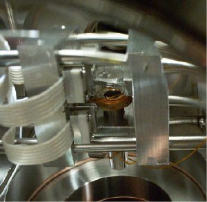
The MIT team first trapped several million sodium atoms in an ‘optical tweezer’. This focused laser beam induces an electric dipole moment in the atoms, which attracts them to the intense electric field of the laser’s focus. They reduced the power of the laser so that the most energetic atoms could escape and cool down the atoms that remained behind. This technique is called ‘evaporative cooling’.

Ketterle and co-workers then transferred the condensate to a special ‘gravito-magnetic’ trap that confines the atoms. The resulting partially condensed gas cloud contained about half a million atoms and had a temperature of about 30 nK. They then weakened the gravito-magnetic trap and this cooled the gas further in a process known as ‘adiabatic decompression’. The temperature of the condensate, at that point containing about 200 000 atoms, dropped below 3 nK.

“It is the same physics behind a pressure cooker,” explained team member Aaron Leanhardt. “If you compress a gas, that is make the confinement stronger, you heat it up. But if you allow the gas to expand by weakening the confinement you cool it down.”

The group then performed another cycle of evaporative cooling to lower the temperature of the cloud even more. This reduced the number of atoms in the condensate to only 30 000 and resulted in a temperature of below 1 nK. The lowest temperature the team measured was 450 pK.

The researchers point out that they could achieve lower temperatures by further weakening the trap and reducing the number of atoms, but admit that this would be “challenging and technically difficult”. As well as practical applications –such as improving atomic clocks and interferometers – they are interested in studying how these ultracold atoms interact with room temperature surfaces. Theory predicts that they should undergo quantum reflection.

Carbon dating confirms origins of biblical tunnel

To date the tunnel, the researchers measured samples of plants and wood contained within the plaster that lined the tunnel. Living plants contain a certain amount of radioactive carbon-14 that is replenished through the process of photosynthesis. Since this quantity starts to diminish once the plant dies, the ratio of carbon-14 to stable carbon-12 reveals how long the plant has been dead.

Frumkin and colleagues measured the relative masses of the carbon isotopes within the plaster using an accelerator mass spectrometer at Oxford University. They calculated that the material in the plaster dates from between about 800 to 510 BC.

The geologists then dated stalactite material – known to have formed after the tunnel was built – from the ceiling of the tunnel. They used uranium-thorium dating by thermal ionization mass spectrometery at the Open University in the UK. This method is based on the detection of both the parent (uranium-234) and daughter (thorium-230) products of decay by the emission of an alpha-particle. The decay of uranium-234 to thorium-230 is part of the much longer decay series that begins in uranium-238 and ends in lead-206

For this technique to work, researchers must know or calculate the initial ratio of thorium-230 to uranium-234 when the sample formed. With time, thorium-230 accumulates in the sample through radioactive decay. They calculate the sample’s age by the difference in the initial ratio of thorium-230 to uranium-234 and the one in the sample being dated.

Frumkin and colleagues found that the stalactites were more than 2300 years old. They therefore conclude that the tunnel could not have been built as late as the 2nd century BC, as some archaeologists believe.

“This is the first time a structure mentioned in the Bible has been radiometrically dated,” Frumkin told PhysicsWeb. “Our dating agrees well with that of the reign of King Hezekiah. Until now this presumption was based only on the biblical text and on the inscription found on the tunnel itself.”

The team now hopes that their technique will be used to date other historical and biblical structures.

Edward Teller dies

Teller was born in Budapest, Hungary, in 1908. In 1930 he received a PhD in physics from the University of Leipzig in Germany, and then left Nazi Germany for Denmark. After working with Neils Bohr in Copenhagen and then living in England, he moved to the US in 1935. He carried out research for several years as a theoretical physicist and then in 1943 went to work on the Manhattan project at the Los Alamos Laboratory in New Mexico.

After the Second World War he concentrated on developing the hydrogen bomb, which had been proposed during the war to exploit the energy resulting from the fusion of light atoms. In 1952, the first explosion from such a bomb took place at the Eniwetok Island in the Pacific, and in the same year the Lawrence Livermore National Laboratory, as it is now known, was founded by Teller and Ernest Lawrence to develop the hydrogen bomb.

Teller was director of Lawrence Livermore from 1958 to 1960, and then served as associate director for physics until his formal retirement in 1977. He was appointed emeritus director of the lab and senior research fellow at the Hoover Institution, positions that he held until his death. In the 1980s he advocated the development of a ballistic missile defence system. Teller received numerous awards during his career, including the prestigious Presidential Medal of Freedom, awarded to him this year by President Bush.

Gold lights up biological cells

It is difficult to detect individual molecules in biological tissue samples, especially using optical methods, because the signal from the molecule of interest must be extracted from that of all the other billions of molecules in the sample. Researchers have got round this problem by attaching a label to the relevant molecule and measuring the intense signal produced by it. But the traditional type of label – fluorescing particles known as fluorophores – can transform into non-fluorescing compounds over time and therefore become useless.

To overcome this, researchers use metallic particles instead of fluorophores. These particles are able to deflect laser light in a process known as Rayleigh scattering. However, because the scattering decreases as the diameter of the particle becomes smaller, methods based on measuring this effect only work with particles that have diameters of at least 40-nm.

To image on smaller scales, Lounis and co-workers stained membrane proteins of COS7 cells with 10-nm gold particles, and then illuminated the sample with light from a 514-nm wavelength argon laser. The laser light was strongly absorbed by the gold nanoparticles, causing the area around them to heat up and the local value of the refractive index to decrease. The researchers then used a second laser beam to detect this change in refractive index.

The Bordeaux team found that the strength of the signal from the individual nanoparticles depends linearly on the intensity of the laser beam used to heat the sample. A 150 nanowatt beam resulted in a signal-to-noise ratio of more than 20, twice as high as the ratio obtained using previous methods. However, Lounis and co-workers admit that the heating effect of their technique may make it unsuitable for imaging living cells – a signal-to-noise ratio of 10 means a temperature rise of about 15 K. They now hope to reduce the heating power in future experiments.

Copyright © 2026 by IOP Publishing Ltd and individual contributors