One of RHIC’s main goals is to produce a quark-gluon plasma – the state of matter that is thought to have existed just millionths of a second after the big bang. Quarks are normally confined in neutrons, protons and other composite particles by the strong force, which is carried by gluons. In a quark-gluon plasma, however, the quarks are free to move throughout the plasma. By studying the properties of the quark-gluon plasma as a function of temperature, energy and particle densities, and entropy, physicists hope to learn more about the strong force and the origins of the universe.
Earlier this year the CERN particle physics laboratory in Geneva reported evidence for quark-gluon matter, but stopped short of claiming that it had seen a quark-gluon plasma. The first RHIC collisions – between beams of gold nuclei with 30 gigaelectron volts (GeV) per nucleon – are four times more energetic than the collisions at CERN. The machine consists of two separate accelerator rings, both 2.4 miles in circumference, that collide beams at six points. RHIC should eventually be capable of beam energies of 100 GeV per nucleon – about ten times the CERN energy.
S Heinze and co-workers from the University of Hamburg and X Nie and colleagues from the Forschungszentrum Jülich have used “spin-polarized scanning tunelling microscopy” to image an antiferromagnetic layer of manganese atoms on a tungsten substrate. In antiferromagnetic materials, the direction of the magnetic moment alternates from one lattice site to the next, but there is no overall magnetization. This has made it difficult to study the magnetic structure of antiferromagnets with existing optical and X-ray techniques.
The German researchers coated the tip of a scanning probe microscope with a ferromagnetic material that emitted spin-polarized electrons. The current that tunnels from the tip to the sample depends on the relative orientation of the magnetization of the tip and the sample. It can therefore provide information about the properties of the layer of manganese atoms. By supplying information at such high resolution, the technique could be used to study in detail the magnetic structure inside antiferromagnetic domain wells, at steps and near impurities or defects. It could also be used to study the antiferromagnetic structure of magnetic surfaces and surface alloys.
The researchers used eight ceramic tips that were connected via a cantilever array to an atomic-force microscope. The tips were coated with a molecular ink such as 1-octadecanethiol that diffused from the tip onto the gold substrate. The ink reacts with the gold to produce a stable monolayer structure on the substrate. A pattern can then be created by moving the microscope stage on which the substrate was attached.
One tip, designated the lead pen, was equipped with force sensors that monitored its position and controlled the width of the pattern. The other “writing” tips then simultaneously reproduced elsewhere on the surface the pattern generated by the lead pen. The researchers used their technique, which is known as “dip-pen nanolithography”, to draw lines, squares and hexagons, but in principle any pattern could be created. The technique can even be used to draw customized nanostructures made of different inks. “This work opens avenues for researchers to begin using dip-pen nanolithography and conventional atomic-force microscopy to do high-resolution and aligned patterning of nanostructures on a large scale that is automated and moderately fast,” say Hong and Mirkin.
Gaidos and Nimmo say that the tidal forces from Jupiter can cause regions of ice near a fault or defect to move relative to one another. This relative motion causes frictional heating that increases the local temperature of the ice and makes it less viscous. This “warm ice”, which is estimated to have a temperature of about 273 K, then flows upwards by a few tens of centimetres over the course of one tidal cycle. “We suggest that such motion over the course of many cycles could be responsible for the formation of structures such as ridge pairs,” say the researchers. Their model predicts pockets of liquid water near the moon’s surface, which would, however, refreeze within tens of years.
In 1960 von Bekesy published the results of his classic measurements on the cochlea, which suggested that the ear was essentially a linear device. However, von Bekesy conducted his experiments on cadavers, and more recent experiments on live cochleas suggest that hearing is essentially nonlinear. The nonlinearity is thought to arise from a biological power supply that leads to positive feedback within the cochlea. Indeed, experiments have revealed a variety of different and seemingly unrelated nonlinear behaviours in human hearing. Moreover, the response of the cochlea remains nonlinear for even the faintest of sounds.
The IMEDEA-Rockefeller team claim that these phenomena can all be explained in terms of solutions to the Hopf equation, a simple-looking nonlinear first-order differential equation that is widely studied for its dynamical properties. For certain values of the control parameter in the Hopf equation, the solutions to the equation exhibit compression of the dynamic range, sharp tuning for small inputs and broad tuning for large inputs – features also observed in human hearing. The next challenge, both theoretically and experimentally, is to link this macroscopic view of the ear to the microscopic behaviour of the individual hair cells in the cochlea.
The new Buyer’s Guide contains information on a wide range of physics equipment: cryogenics, lab electronics, lasers, magnets, microscopy, power supplies, test & measurement and vacuum are just some of the categories included in the Buyer’s Guide. More than 2000 companies are listed in the guide, and a sophisticated search facility makes it easy to research new products and services, or request additional information. Check the Buyer’s Guide out for yourself at physicsweb.org/buyers/.
Another improvement is that access to all the articles on PhysicsWeb is now free – which is why the buttons for News, Reviews and Physics World on the left of the screen have changed from red to blue. Observant users will notice that one of the buttons – Member Services – has remained red. This is because these services – such as the on-line change-of-address form – are only relevant to members of the Institute of Physics. If you want more information about joining the Institute click here.
“Science is more controversial than art can ever be.” Strange words for an artist, perhaps, but Cornelia Parker has been inspired by science for many years. Indeed, Parker’s “Cold, dark matter” – the suspended remains of a garden shed that the army blew up on her behalf – is currently on show at the recently opened Tate Modern gallery in London.
Parker is one of a growing number of artists who have realized that science is fertile territory for the imagination. Of course, in the past painters and sculptors such as Leonardo da Vinci were active in science, but in an otherwise increasingly specialized world, more and more contemporary artists are linking up with scientists.
One of the many new collaborations is centred around CERN, the European laboratory for particle physics in Geneva. CERN is collaborating with the London Institute, the world’s largest college of art, design and communication, on a project called “Signatures of the invisible”. Leading European artists, including Turner prize-winners Richard Deacon and Anish Kapoor, will spend up to two months working with physicists from CERN to create works of art that will be shown in major galleries around the world.
Common beauty
So what does CERN hope to gain from the collaboration? “I am a strong believer in bringing people together over obvious divides in order to weaken those divides, be they political or cultural,” says Maurice Jacob, former head of the lab’s theory division and one of the founders of the project. “There are many obvious differences between art and science,” he says, “but also many common points.”
One of the artists involved in “Signatures of the invisible”, Monica Sand from Sweden, has been collaborating with CERN for the past eight years, and has mounted several exhibitions of sculptures that incorporate research results. “My main interest is space, and how light shapes space,” she says.
In a work called “Traces” Sand explores the idea that an elementary particle is never seen directly. Instead, physicists infer the existence of an elementary particle from the traces of other particles that have been disturbed in its wake. “How is one to know which knowledge is required to interpret the traces?” she asks. She explores the question through sculpture made from materials used to track particles – scintillators and wavelength shifters.
“Science and art are two different approaches that complement each other, and [both] are needed to produce a balanced vision of the world,” says physicist and science writer F David Peat. “They also have much in common. Science is very much directed by aesthetics and beauty – notions of what fits, economy of means, and ideas of form and order. The same issues surface, in different ways, in art.” But there are differences. “Science boasts of being objective and value free,” Peat says, “while art is concerned with value and human response.”
Peat has collaborated with a number of artists, including Anthony Gormley and David Hockney. “These people think deeply about issues that also interest scientists,” he says. “But the fact that they are not scientists is what is important, because they bring a different perspective.”
Sentimental rubbish?
Cornelia Parker’s irreverent style appealed to Nature editor Philip Campbell, who discreetly inserted images of her work into the magazine to see how readers would react. One of the images looked like an electron micrograph but was, in fact, a close up of the grooves on a record owned by Hitler. Campbell admits that Parker’s work did not cause the stir he was hoping for because it actually blended in too well. Nevertheless he subsequently published a series of articles on art and science by art-historian Martin Kemp and would like to see more art on the pages of Nature in the future.
Such link ups between art and science are important, says Ken Arnold of the biomedical research charity the Wellcome Trust. He feels that collaborations lead to greater self-awareness in scientists and artists through the need to explain things to someone with a different intellectual viewpoint.
Wellcome runs a “SciArt” scheme to encourage artists and scientists to “look beyond the traditional boundaries of their professions for mutual benefit”. This year it awarded 11 grants totalling £200 000. Arnold believes that the projects funded by Wellcome should also encourage the public appreciation of science.
But not everyone is so enthusiastic. “Absolute junk. Sentimental rubbish,” says biologist and media science pundit, Lewis Wolpert. “To say there is a lot in common between science and art is rubbish. We can say that we understand biology better than we did 30 years ago, but there is no such thing as progress in art.”
Nor is art a good way to promote science, according to Wolpert: “Anyone else – playwrights, writers, bankers – could improve the public understanding of science, but not artists. If you want to help art, then sure, bring in science. But nothing will happen the other way around.” He adds that he cannot think of a single instance in which art has helped the creative process in science. Not surprisingly, Wolpert “attacks the Wellcome Trust constantly” over the money it spends on the SciArt scheme.
Peat, however, makes the claim that the American artist Charles Biederman provided the late David Bohm with insights into physics. “Bohm was seeking a new order to physics, one compatible with quantum theory,” says Peat. “He rejected the old ‘Cartesian order’ based on points in a continuous space and looked instead to algebraic and topological structures.”
For many years Bohm exchanged ideas with Biederman, who was interested in structure and order in art and who studied Cezanne’s paintings extensively. “Bohm once said that if he could only describe such a painting in mathematical terms, it would be the exact mathematics he needed for quantum theory,” says Peat.
In another case of art leading science, the painter Jackson Pollock was unknowingly exploring fractals and chaos in his abstract drip paintings long before they were recognized by mathematicians. Now John Barrow, a cosmologist at Cambridge University, has joined forces with Martin Kemp and artist Richard Bright to explore new ways of representing higher-dimensional space. The trio has been awarded a Wellcome grant to investigate the hypothesis that perspective, which has served as a visual aid in almost every field of science until the present, is actually limiting the ability of scientists to represent complex spaces.
Geometric art
Maths and physics also come together with art in the work of Simon Thomas, a sculptor who is interested in exploring “the efficiencies of space”. Thomas was artist-in-residence in the physics department at Bristol University for two years and is currently working on a cone-like sculpture in honour of Paul Dirac. The sculpture, which was commissioned by Institute of Physics Publishing (the publishers of Physics World), will sit outside the @Bristol science centre. Built up from layers of crosses that become progressively shallower, the sculpture poses the question: what happens when we get to the Planck scale?
Thomas has also collaborated with the mathematicians Andy Burbanks and Neil O’Connell at Hewlett-Packard in Bristol on a project to explore the interface between maths and art. In the course of the project, Thomas tried to develop a “more analytical approach” to art, and created a set of geometric sculptures that were later distributed around the research labs.
Jeremy Gunawardena, director of Hewlett-Packard’s Basic Research Institute in Mathematics, says the $75 000 project was well worth the money and that it helped to break down the “tunnel vision” that takes hold in research labs. “People have been surprised at how well the project has worked,” he says. “Having the sculptures has created a different feeling in the building. It makes you realize that we live in a much more complex space than just a technology lab. Art and aesthetics are important.”
But not all collaborations between artists and scientists will meet with such success. F David Peat, for instance, thinks that art-science collaborations are becoming too fashionable and that a lot of money is being poured into the field to produce what are only mediocre results.
Ken Arnold at Wellcome agrees that a lot of work in this area is not very good, and predicts that art-science projects will become less popular in the future. However, he thinks that is important for specialists to be able to “peer into” other disciplines.
“We live in a specialist world,” says Arnold. “The idea that we can return to the Renaissance is foolhardy. But hopefully in the future we will have more open-minded scientists and artists.”
The geometry of the universe is Euclidean and space is flat. This has now been confirmed from detailed measurements of the cosmic microwave background – the radiation left over from the big bang – by an international team of astronomers from Italy, the UK, the US, Canada and France. The Boomerang collaboration, led jointly by Paolo de Bernardis of the University of Rome and Andrew Lange of the California Institute of Technology, has measured the angular distribution of temperature fluctuations in the microwave background with unprecedented accuracy. Such fluctuations contain information about the energy density and curvature of the universe (P de Bernardis et al 2000 Nature404 955).
Einstein’s general theory of relativity predicts that gravity is, in effect, a curvature of space. This means that we can replace the gravitational field of the Sun by a slight curvature in the surrounding Euclidean space. The effect of this is that straight lines, as traced by light rays from distant stars, are no longer straight.
The deviation, which is tiny, was first observed in 1919 during a solar eclipse. The measurements showed that light from a distant star near the edge of the Sun was deflected by just 2 seconds of arc. This observation revolutionized modern physics.
Overnight, a new theory of one of the fundamental forces of nature was accepted. We had to abandon our precepts about the geometry of the universe being Euclidean.
Parallel lines were no longer parallel. Moreover, gravity could now explain one of the most challenging problems in physics – the origin of the universe.
The big-bang theory was a consequence of the theory of gravitation. The universe expanded in a precarious competition between the kinetic energy of the expansion and the gravitational potential energy that threatens to eventually cause the universe to contract. If there is enough matter in the universe, then gravity will dominate, the universe will decelerate and it will begin to contract. However, if the density of matter is below a critical value, called Wcritical by cosmologists, then the universe will expand forever.
The critical density is well known and is given by 3H02/8pG, where G is the gravitational constant and H0 is the Hubble constant, which has recently been measured to an accuracy of 10%. But what is not known is the actual density of the matter, most of which is known to be non-luminous or “dark” and thus exceedingly difficult to detect.
Geometry, matter density and dark energy
There are, in fact, three possibilities for the geometry of the universe. It could be flat (or Euclidean) and resemble a sheet in 2-D. Alternatively it could have a spherical geometry and look like the surface of a sphere, or it could be hyperbolic and resemble a saddle-shaped surface in 2-D. Each geometry offers an unbounded space that encompasses the entire universe.
General relativity predicts that if the universe is below the critical density, it will expand forever and have a hyperbolic geometry. Such a subcritical universe has a “positive” energy, which means that the kinetic energy associated with its expansion is much greater than its gravitational potential energy. In contrast, a universe in which the density of matter is greater than Wcritical has a negative total energy. Meanwhile, a critical-density universe has zero energy. Einstein’s theory identifies the energy of the universe with the nature of its geometry. Only a critical-density universe is Euclidean.
Observations strongly hint that the matter density is subcritical. Although about 90% of this matter is dark, its gravitational effects allow us to measure its density. A variety of techniques point to a matter density that is one third of the critical value, with an uncertainty of a factor of two at the most. However, we cannot infer that the universe is destined to expand forever. There may also be “dark energy” present, which provides a repulsive force.
The concept of dark energy was originally introduced by Einstein in 1917, some 12 years before Edwin Hubble discovered that the universe is expanding. Einstein conceived the idea to counter the gravitational effect of matter and provide a static universe that neither collapsed nor expanded. He called this repulsive force the cosmological constant, which appeared as an additional constant in the equations of general relativity and had no Newtonian counterpart.
In 1930 Einstein became convinced of Hubble’s expansion law, and later admitted that the introduction of the cosmological constant was one of the greatest mistakes of his life. Meanwhile, others – notably Russian theorist Alexandre Friedmann in 1922 and Belgian cosmologist Georges Lemaitre in 1927 – predicted a universal expansion that culminated in Hubble’s discovery.
However, theory has a habit of rebounding and once Pandora’s box is opened, it becomes hard to close. Dark energy would never be forgotten, and the cosmological constant has regularly resurfaced to account for some particular observational challenge – and has invariably faded away again as observations improved.
The first real revival came from theory. In 1981 inflationary cosmology provided the first major new insight into the big bang since the 1920s. According to this model, the universe underwent a phase transition 10-35 s after the big bang and expanded exponentially in scale for a brief period. This period of rapid expansion flattened the geometry of the universe. Inflation predicts that the universe is at the critical density. Dark matter could not account for the critical energy, and the cosmological constant remained the plausible culprit, if inflation did indeed occur.
Precision measurements
If we could directly measure the geometry of the universe, then we could bypass the dark-matter problem and test the inflationary prediction of flatness. Enter the Boomerang experiment. Designed to study the cosmic microwave background with unprecedented accuracy, this microwave telescope surveyed 2.5% of the sky with an angular resolution of 0.25o during a 10-day balloon flight over Antarctica (figure 1).
One of the key pieces of evidence for the big bang is that the cosmic microwave background has a perfect black-body spectrum with a temperature around 2.73 K in all directions. However, theory predicts that there should be temperature fluctuations at the level of 10-5 in order to seed galaxy formation. Indeed, such fluctuations were discovered in 1992 by the COBE satellite, which had an angular resolution of 7o.
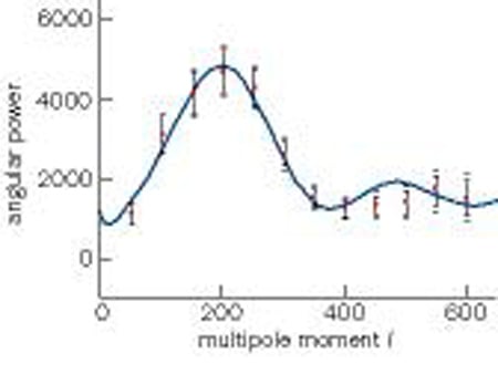
The much higher resolution of the Boomerang experiment has enabled astronomers to make a fundamental test of the nature of the fluctuations. The primordial fluctuations are enhanced by the astrophysics of the early universe on small angular scales. These scales correspond to the maximum distance a fluctuation driven by pressure variations can propagate in the early universe. A peak in intensity occurs on the horizon of the universe 300 000 years after the big bang, when the matter and radiation ceased to interact via photon scattering. In the case of a flat universe, this peak is predicted to occur at a characteristic angular scale of 45 arcminutes.
This physical scale translates to an angular scale in the sky that depends on the curvature of the universe. If the universe is negatively curved, or has a lower density, the predicted peak shifts to smaller angles. In effect, the gravity field of the universe acts like a lens.
Boomerang has measured the peak with unprecedented precision and gives confirmation of the primordial origin of the fluctuations. Moreover, the measured peak agrees precisely with the expectation for a flat universe. The location of the peak means that the density of matter is within 10% of the critical value. The universe must therefore be dominated by dark energy – the modern reincarnation of the cosmological constant.
Tentative measurements of the distances to Type Ia supernovae show evidence that the expansion of the universe is accelerating, as predicted for a universe that is spatially flat but in which two-thirds of the critical density is accounted for by the dark energy associated with the cosmological constant (B P Schmidt et al. 1998 Astrophys. J. 507 46 and S Perlmutter et al. 1999 Astrophys. J. 517 565). Hence cosmologists are happy, and a consistent cosmological model beckons with independent verification of an unexpected key parameter from two totally independent experiments.
Unexpected results
Life would be dull for cosmologists if all that emerged from Boomerang was confirmation of flatness and dark energy. Although the predicted peak at 45 arcminutes is at exactly the angular scale expected for the preferred flat model, the data continue to 15 arcminutes. Theory predicts a second feature due to the wave-like oscillations of the radiation pressure-driven fluctuations. This feature corresponds to the trough of the wave that peaked at 45 arcminutes and shows up in the power distribution as a second peak (figure 2). This second peak is smaller than the first because the radiation is “redshifted” very slightly during the time it takes the trough of the wave to become visible on the horizon of the universe.
The big surprise in the Boomerang data is that the amplitude of the second peak is smaller than predicted, although it appears to occur at the expected position. Within a week of the release of the first Boomerang results, the electronic Web servers buzzed with speculation about why this might be the case. Favourite among the preferred explanations is the idea that the density of ordinary or baryonic matter might be up to twice as large as indicated by the measured abundances of hydrogen, helium and lithium. Increasing the baryon density preferentially damps out the shorter-wavelength pressure waves, and reduces the amplitude of the second peak.
This is not a unique explanation, however, but it does lead to novel predictions. For example, the ratio of baryonic to non-baryonic dark matter is likely to be 25% or more. This suggests that a baryonic “footprint” may show up in galaxy surveys, such as the 2dF surveys on the Anglo-Australian telescope and the Sloan Digital Sky Surveys. Indeed, baryon-induced oscillations are expected to become visible in 3-D galaxy distributions stretching back 330 million light-years.
It seems to be inevitable in astronomy that each new discovery raises further challenges. The universe is flat, but absorbing the full implications of the Boomerang data will take some time, and will undoubtedly inspire new experimental efforts and new insights into the nature of the universe.
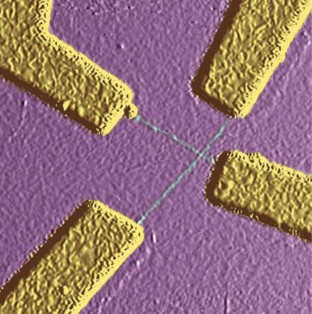
AFM image on a carbon nanotube ‘cross’. The nanotubes are the thin green lines connected to the much larger electrodes.
Nanotechnology is predicted to spark a series of industrial revolutions in the next two decades that will transform our lives to a far greater extent than silicon microelectronics did in the 20th century. Carbon nanotubes could play a pivotal role in this upcoming revolution if their remarkable electrical and mechanical properties can be exploited.
Since the first measurements were made in 1997, these rolled up sheets of graphite have captured the imagination of researchers around the world. Progress in understanding the basic physics and chemistry of nanotubes has advanced at a phenomenal rate – and shows no signs of slowing.
Nanotubes have an impressive list of attributes. They can behave like metals or semiconductors, can conduct electricity better than copper, can transmit heat better than diamond, and they rank among the strongest materials known – not bad for structures that are just a few nanometres across. Several decades from now we may see integrated circuits with components and wires made from nanotubes, and maybe even buildings that can snap back into shape after an earthquake.
Nanotubes as test tubes
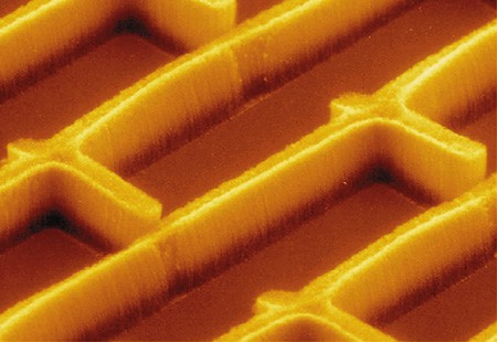
SEM image of carbon nanobrushes made by growing nanotubes vertically on a surface.
Carbon nanotubes were first observed in 1991 by Sumio Iijima at NEC in Japan. These so-called multiwall nanotubes consisted of several concentric tubes of carbon nested inside each other. Two years later Iijima, Donald Bethune at IBM in the US and others observed single-wall nanotubes just 1-2 nm in diameter. But the field really took off a few years later when various groups found ways to mass-produce high-quality nanotubes.
Paul McEuen describes how the remarkable electrical properties of single-wall nanotubes stem from the unusual electronic structure of graphite. A nanotube can be either a metal or a semiconductor depending on the way the graphite sheet is rolled up. Metallic nanotubes are also ideal systems in which to explore electron transport in one dimension thanks to their near-perfect structures.
Other fundamental phenomena in quantum physics can be tested on multiwall nanotubes, as Christian Schönenberger and Lazslo Forró explain. Researchers expect to find more complex behaviour for multiwall nanotubes due to the interactions between adjacent layers.
Applications and challenges
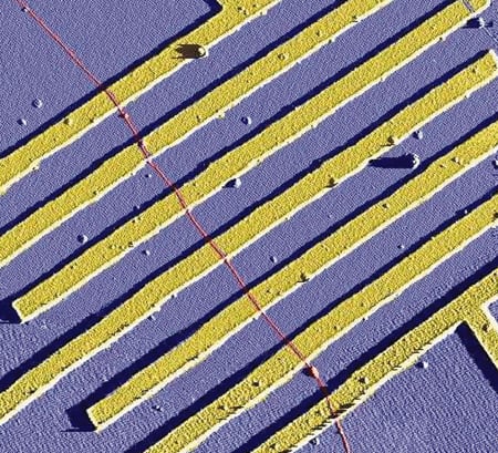
AFM image of a single carbon nanotube on electrodes. The nanotube is the thin red line.
Industry has begun to notice the unique properties of carbon nanotubes, as Walt de Heer and Richard Martel report. The first commercial device that uses multiwall nanotubes may be a lamp that operates on the field-emission principle. Moreover, the field-emitting characteristics of carbon-nanotube films have attracted serious interest from the giants of the display industry. Samsung, for example, plans to market a flat-panel colour display made from multiwall nanotubes within two years. Meanwhile, research at IBM indicates that nanotubes transistors should be competitive with state-of-the-art silicon devices. Nanotubes could also be used to store hydrogen to power electric vehicles.
However, many technological hurdles need to be overcome before large-scale applications reach the marketplace. For example, the techniques that are used to build electronic components from nanotubes are painstaking and utterly inappropriate for mass production. But perhaps the most severe limitation is that high-quality nanotubes can only be produced in very limited quantities – commercial nanotube soot costs 10 times as much as gold!
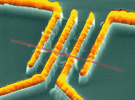
SEM image of a multiwall nanotube lying across four gold electrodes.
Hongjie Dai describes how researchers are learning to control the growth of carbon nanotubes, and manufacture them more efficiently. These techniques have produced ordered nanostructures with advanced properties.
Although there are many challenges ahead, nanotubes appear destined to open up a host of new practical applications and improve our understanding of basic physics at the nanometre scale.
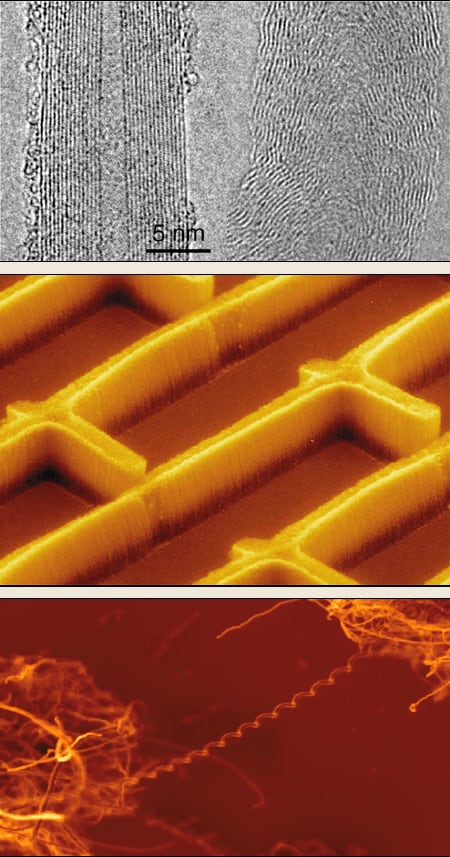
1 Nanotube structures (a) Multiwall carbon nanotubes are composed of concentric sets of single-wall tubes and have typical outer diameters of 10–50 nm. This structure can be seen clearly in this high-resolution transmission electron microscope image of a multiwall nanotube grown in an arc discharge (left), whereas other growth techniques produce less ordered structures (right). Images by Jean-Marc Bonard and co-workers at EPFL. (b) A scanning electron microscope image of a ‘nanobrush’ of vertically aligned nanotubes obtained by printing a catalyst on a substrate: the nanotubes only grow at the catalyst sites (by the thermal decomposition of a reaction gas). This structure was produced by the groups of Hannes Kind and Laszlo Forró at EPFL, and Louis Schlapbach at the University of Fribourg. (c) By adjusting the growth parameters, different forms of nanotubes, such as these spirals grown by Schlapbach’s group, can be produced.
In 1991 Sumio Iijima used a high-resolution transmission electron microscope to study the soot created in an electrical discharge between two carbon electrodes at the NEC Fundamental Research Laboratory in Tsukuba, Japan. He found that the soot contained structures that consisted of several concentric tubes of carbon, nested inside each other like Russian dolls.
A year later Thomas Ebbesen and Pulickel Ajayan, also working for NEC in Tsukuba, developed a highly efficient way of making large quantities of these multiwall nanotubes. Subsequently, in 1993, Iijima’s group at NEC and Donald Bethune’s group at IBM’s Almaden Research Center in California independently discovered single-wall nanotubes. Whereas the multiwall nanotubes were tens of nanometres across, the typical diameter of a single-wall nanotube was just one or two nanometres. The past decade has seen an explosion of research into both types of nanotube.
Today, nanotubes can be grown efficiently by the catalytic decomposition of a reaction gas that contains carbon, with iron often being used as the catalyst. This process has two main advantages. First, the nanotubes are obtained at much lower temperature, although this is at the cost of lower quality. Second, the catalyst can be grown on a substrate, which allows novel structures, such as “nanobrushes”, to be obtained (figure 1). Currently nanotubes can be grown to lengths exceeding 100 microns, and in various shapes such as “nanosprings”.
A nanotube can be considered as a single sheet of graphite that has been rolled up into a tube. The electronic properties of the resulting nanotube depend on the direction in which the sheet was rolled up. Some nanotubes are metals with high electrical conductivity, while others are semiconductors with relatively large band gaps. Nanotubes also have remarkable mechanical properties that can be exploited to strengthen materials or to act as “tips” in scanning probe microscopes. And since they are composed entirely of carbon, nanotubes also have a low specific weight.
Mechanical properties
In a sheet of graphite each carbon atom is strongly bonded to three other atoms, which makes graphite very strong in certain directions. However, adjacent sheets are only weakly bound by van der Waals forces, so layers of graphite can be easily peeled apart – as happens when writing with a pencil. As we shall see, it is not so easy to peel a carbon layer from a multiwall nanotube. Carbon fibre is already used to strengthen a wide range of materials, and the special properties of carbon nanotubes mean that they could be the ultimate high-strength fibre.
In 1996 Michael Treacy and Ebbesen, now at NEC Research in Princeton, and Murray Gibson from the University of Illinois in Urbana, measured the Young’s modulus of multiwall nanotubes. The Young’s modulus of a material is a measure of its elastic strength. Treacy and co-workers arranged multiwall nanotubes vertically on a surface so that the tubes were fixed at the bottom and free to move at the top, and then used a transmission electron microscope (TEM) to measure the thermal vibrations of the free ends. The measured vibration amplitude revealed an exceptionally high elastic Young’s modulus of about 1012 newtons per square metre (or one terapascal) – about five times the value for steel.
It is now known that the Young’s modulus should approach a value of 1.25 terapascals. This is true both for multiwall and single-wall nanotubes because the modulus is mainly determined by the carbon-carbon bonds within the individual layers. This value has recently been confirmed by Charles Lieber and co-workers from Harvard University, who used a scanning force microscope (SFM) to bend nanotubes that were mechanically fixed at one end. The scanning force microscope can image, manipulate and measure the force needed to bend the tubes.
The bending stiffness can also be measured by placing the nanotubes across “nanopores” and using an atomic force microscope to bend them in the middle – a technique developed by Jean-Paul Salvetat and co-workers from the École Polytechnique Fédérale de Lausanne (EPFL) in Switzerland. Salvetat and co-workers began by depositing nanotubes from a liquid onto a well-polished alumina membrane that contained pores about 200 nm across (figure 2). Occasionally a nanotube spanned one of the pores and the microscope was used to measure how the deflection, which is inversely proportional to the Young’s modulus, varied with the applied force.
Salvetat and co-workers found that multiwall nanotubes grown by arc discharge had a modulus of about 1 terapascal, whereas those grown by the catalytic decomposition of hydrocarbons had a modulus that was smaller by one to two orders of magnitude. These results demonstrate that only highly ordered and well-graphitized nanotubes have a stiffness comparable to graphite, whereas those grown by catalytic decomposition have many more defects. (By well graphitized we mean that the carbon-carbon bonds within each layer are strong, while the interactions between layers are weak.) TEM images indeed reveal that the carbon sheets are neither continuous nor parallel to the tube axis.
Lieber and co-workers went on to explore larger forces and deformations, and compared carbon nanotubes with nanorods made from silicon carbide, another very strong material. What they found was surprising: whereas the silicon-carbide nanorods eventually fractured, the multiwall carbon nanotubes buckled, but did not break. This behaviour has since been confirmed in several experiments in which the nanotubes are either bent or compressed along their length.
2 Bending and stretching nanotubes (a) An atomic force microscope (AFM) image of a multiwall nanotube across a pore. The AFM can also be used to apply a force to the nanotube and measure how much it bends, which allows the Young’s modulus to be determined. (J-P Salvetat et al. 1999 Adv. Mat.11 161; Phys. Rev. Lett.82 944) (b) Scanning electron microscope images of a multiwall nanotube held between two AFM tips. When the tips are pulled apart the outermost layer of the nanotube ruptures (see Yu et al. in further reading).
Euler was the first to calculate what happens to a rod when it is compressed along its length (so-called axial compression). Initially the rod remains straight as the compression increases, before flipping into a curved form at the Euler limit. If this experiment is performed with a drinking straw at constant load, the straw will suddenly develop kinks, which remain if the load is removed. In other words, the kinks are plastic rather than elastic deformations.
Carbon nanotubes are different: first they will bend over to surprisingly large angles, before they start to ripple and buckle, and then finally develop kinks as well. The amazing thing about carbon nanotubes is that these deformations are elastic – they all disappear completely when the load is removed.
To see how these properties might be useful, imagine owning a BMW car made from carbon nanotubes and being unlucky enough to crash into a wall. Due to the high force of the impact, the nanotubes would bend and then buckle, squeezing your BMW into the shape of something like a Volkswagen Beetle. This would happen over a relatively long distance, which would provide an effective “crunch zone”. Moreover, after the crash all the buckles and kinks would unfold and your BMW would “reappear” as if nothing had happened! To be completely safe, however, the nanotubes would have to be combined with energy-absorbing materials, otherwise the collision between the car and the wall would be completely elastic and you would rebound from the wall with the same speed as you hit it!
Other, less futuristic applications might include lightweight bullet-proof vests and earthquake-resistant buildings, while nanotube tips for scanning probe microscopes are already commercially available.
Further insights into the mechanical properties of multiwall nanotubes emerged recently when Rodney Ruoff of Washington University in St Louis and co-workers attached the ends of a multiwall nanotube to a pair of AFM tips and stretched it until it broke (figure 2). They found that the tensile strength was at least an order of magnitude lower than would be expected if the stress was uniformly distributed over all the layers of the nanotube. The outermost layer had to take most of the stress because the tips only made contact with the outside of the nanotube. Ruoff and co-workers found that the outermost tube ruptures at the tensile limit, and that this is followed by a sudden elongation. From TEM images, they concluded that the ruptured outer tube then slides over the inner tubes.
The high strength of carbon nanotubes makes them promising candidates in reinforcement applications, but there are many outstanding problems that must be overcome. First, the properties of the individual tubes must be optimized. Second, the tubes must be efficiently bonded to the material they are reinforcing (the matrix) so that they actually carry the loads. Third, the load must be distributed within the nanotube itself to ensure that the outermost layer does not shear off.
Electronic properties
Carbon nanotubes are giant molecular wires in which electrons can propagate freely, just as they do in an ordinary metal. This contrasts strongly with conventional “conducting” polymers in which the electrons are localized. These molecules are actually insulators and only become conductors if they are heavily doped. Graphite, on the other hand, can conduct electricity because one of the four valence electrons associated with each carbon atom is delocalized and can therefore be shared by all the carbon atoms.
However, it turns out that a single sheet of graphite (also known as graphene) is an electronic hybrid: although not an insulator, it is not a semiconductor or a metal either. Graphene is a “semimetal” or a “zero-gap” semiconductor.
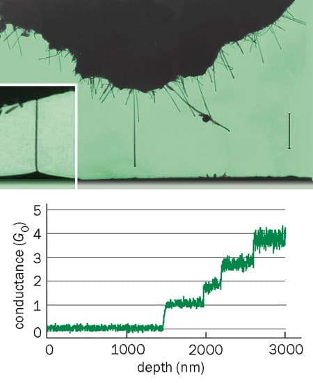
3 Quantized conductance (a) A transmission electron microscope image of the macroscopic fibre of multiwall nanotubes used by Walt de Heer and co-workers at the Georgia Institute of Technology to measure the conductance of individual multiwall nanotubes. As the fibre is lowered into liquid mercury, contact will initially be made with just one of the nanotubes that sticks out from the bundle (insert). (b) A plot of conductance versus depth clearly shows that the conductance increases in units of the quantum of conductance. G0=2e2/h, as the number of individual nanotubes making contact with the mercury increases. This suggests that nanotubes are ideal waveguides for electrons (see Frank et al. in further reading)
This peculiarity means that the electronic states of graphene are very sensitive to additional boundary conditions, such as those imposed by rolling the graphene into a tube. It can be shown that a stationary electron wave can only develop if the circumference of the nanotube is a multiple of the electron wavelength. This boundary condition means that a nanotube is either a true metal or a semiconductor – a fact that has been confirmed in experiments with single-wall nanotubes.
One would expect to find more complex behaviour for multiwall nanotubes because of interactions between adjacent layers, and this is the subject of ongoing research. Moreover, by combining different nanotubes, and supplementing them with gate electrodes, there is the potential to make a wide variety of electronic devices, ranging from quantum wires to field effect transistors.
On the fundamental side, a perfect metallic nanotube should be a ballistic conductor: in other words, every electron injected into the nanotube at one end should come out the other end. Although a ballistic conductor does have some resistance, this resistance is independent of its length, which means that Ohm’s law does not apply. Indeed, only a superconductor (which has no electrical resistance whatsoever) is a better conductor.
A defect-free carbon nanotube is like an optical fibre. Fibres with large cores are called multi-mode fibres because several wavelengths (or eigenmodes) are allowed to propagate, usually at different speeds, along the fibre. For data transmission, so-called single-mode fibres are preferred because they allow for higher data rates. A single-wall nanotube is almost a single-mode fibre for electrons. Theory predicts the existence of two propagating eigenmodes for a single-wall nanotube, independent of its diameter. The electric conductance (the inverse of the resistance) is then expected to be twice the fundamental quantum of conductance, G0 = 2e2/h, where e is the charge on the electron and h is the Planck constant. This means that nanotubes are predicted to have a minimum resistance of about 6500 Ohms, independent of their length.
One-dimensional conductors are also predicted to have unusual electronic properties that cannot be explained by Fermi-liquid theory – the theory that can predict the properties of most materials. Here, we will concentrate on two recent experiments that address the question of whether multiwall nanotubes are ballistic or diffusive conductors.
In 1998 Walt de Heer and colleagues at the Georgia Institute of Technology in the US invented an ingenious way to measure the electrical conductance of multiwall nanotubes. A macroscopic fibre of multiwall nanotubes was gently lowered into a drop of liquid metal (figure 3). Because individual nanotubes stick out from the fibre, it is possible, by dipping the nanotubes to different depths, to determine the resistance of individual nanotubes. This technique also allows any variation of resistance with length to be detected.
4 In contact with nanotubes A scanning electron microscope image of a multiwall nanotube lying across four gold electrodes, which were fabricated by state-of-the art electron-beam lithography prior to the deposition of the nanotube. (Courtesy: C Schönenberger and A Bachtold)
This method for making electrical contact with nanotubes is very different to techniques that rely on sub-micron fabrication technology (see, for example, figure 4). Quantized conductance will only be observed if ideal contacts are made to the nanotube, and these can be very difficult to achieve. (In an ideal contact none of the electrons entering or leaving the nanotube will be backscattered by the contact.) Early experiments with microfabricated contacts found strong evidence that electrons were scattered. The transport therefore appeared to be diffusive rather than ballistic.
However, de Heer and co-workers found that all multiwall nanotubes have nearly the same conductance, G0 = 2e2/h, and that the dependence of the resistance on length was very weak. In other words, multiwall nanotubes appeared to be ballistic conductors, despite the interactions expected between the different layers (figure 3).
Moreover, the electrical current that could be passed through a multiwall nanotube corresponded to a current density in excess of 107 amps per square centimetre. If nanotubes were classical resistors, the power dissipated by such a current would heat the nanotube so much that it would vaporize. The fact that this does not happen suggests that the electrons in nanotubes are strongly decoupled from the lattice. “Hot” electrons are efficiently removed by the liquid-metal contact rather than being converted into lattice vibrations.
Since multiwall nanotubes consist of several concentrically arranged single-wall nanotubes, one would not expect them to behave as one-dimensional conductors. If adjacent carbon layers interact as in graphite, electrons would not be confined to one layer. The results from de Heer and co-workers suggest, however, that the current mainly flows through the outermost layer, and experiments by the authors in Basel and at EPFL confirm this. It appears therefore that the inner layers only provide mechanical support, although this might change if we were able to make electrical contact with all the layers. However, the question of whether the electron transport is ballistic or diffusive remains unresolved.
Nanotubes and magnetic fields
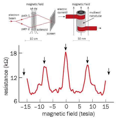
Nanotubes have also been used to help demonstrate the Aharonov-Bohm effect, one of the most fundamental phenomena in quantum physics. In the Aharonov-Bohm effect a beam of quantum particles, such as electrons, is split into two partial beams that pass on either side of a region containing a magnetic field, and these partial beams are then recombined to form an interference pattern. The interference pattern can be altered by changing the magnetic field – even though the electrons do not come into contact with the magnetic field (figure 5).
The observation of the interference pattern demonstrates that a single electron does not choose a particular path but behaves as an extended wave and follows both paths simultaneously. The interference pattern shifts as the magnetic field changes, returning to the original pattern when the magnetic flux has changed by the quantum of magnetic flux, f0 = h/e.
5 The Aharonov-Bohm effect with nanotubes (a) In the standard Aharonov-Bohm effect the magnetic flux through the solenoid changes the relative phase of the electron waves in paths 1 and 2, leading to the formation of an interference pattern on the screen. When the flux is changed, the interference pattern shifts on the screen. (b) In a carbon magnetic field (tesla) nanotube, the two paths are clockwise and anticlockwise around the nanotube, and the shift in the interference pattern manifests itself as a change in the electrical resistance along the nanotube as a function of magnetic field (c). The magnetic field at the peaks can be related to the quantum of magnetic flux, h/2e, and the cross-section of the nanotube (see Bachtold et al. and Schönenberger et al. in further reading)
The Aharonov-Bohm effect is particularly interesting because it depends on the electromagnetic vector potential, A, which is related to the magnetic field, B, through the equation, B = curl A. Originally it was thought that the vector potential, A, did not have a physical meaning (various quantities can be added to A without the value of the physical observable, B, being changed). However, the theoretical prediction of the Aharonov-Bohm effect, and its subsequent confirmation in experiments, showed that this is not the case.
Imagine a carbon nanotube placed in a magnetic field with its axis parallel to the field (figure 5). Since nanotubes are cylindrical conductors, the electrons can propagate in either the clockwise or the anticlockwise direction. These two “paths” interfere, resulting in a periodic modulation of the electrical resistance as the magnetic flux through the tube is changed. In this case the period is f0/2 = h/2e. This effect is relatively robust and can be observed even if the electron transport in the nanotube is diffusive.
Last year a collaboration between the authors’ groups at Basel and the EPFL measured the electrical resistance of multiwall nanotubes as a function of temperature and magnetic flux. There was a resistance peak at B = 0, and smaller peaks at B = ±8.5 T, in good agreement with the predictions of the Aharonov-Bohm effect.
Moreover, the value of the magnetic field at the peaks showed that the current was carried by the outermost layer of the nanotube. We note that the magnetic flux through the tube is simply the product of the magnetic field and the cross-sectional area of the tube. The separation of the peaks, DB, and the nanotube radius, r, are therefore related by a simple equation: DB = h/(2epr2). For DB = 8.5 T we find that r = 9 nm, which agrees with direct measurements of the radius with an atomic force microscope. Since a single-wall nanotube has a radius of just a few nanometres, a much larger magnetic field – much larger than is experimentally possible today – would be needed to observe the effect in this system.
The amplitude of the observed Aharonov-Bohm oscillations suggests that the transport is not ballistic in these experiments: in an ideal ballistic nanotube the difference in the resistance at the peaks and the troughs would be much larger. This is because the relative phase of the wavefunction around the circumference determines whether the nanotube is a metal or a semiconductor. Since the magnetic flux changes the phase, a metallic nanotube should continuously evolve into a semiconducting one and vice versa with a flux period of h/e (i.e. twice the period of the Aharonov-Bohm effect). At low enough temperatures the resistance should approach infinity, as the semiconductor would effectively become an insulator. However, this metal-to-semiconductor transition has not been observed in experiments yet.
This and other magneto-resistance measurements show that the electron transport is diffusive, with the scattering length ranging from 3 nm (very diffusive) to 100 nm (intermediate between diffusive and ballistic). The reason for such a wide range of behaviours is puzzling, as is the fact that the metal-to-semiconductor transition has not been observed.
Although transport in multiwall nanotubes is best characterized as diffusive, large electric currents (up to 1 mA) are observed, demonstrating that the electrons couple only weakly, if at all, to the lattice. All these magneto-resistance measurements can be understood in terms of Fermi-liquid theory by assuming the transport is diffusive in two dimensions. However, recent tunnelling experiments in multiwall nanotubes by our Basel-EPFL collaboration have revealed anomalies similar to those seen in single-wall nanotubes. New approaches that go beyond Fermi-liquid theory, such as the Luttinger-liquid model, will be needed to explain these results.
Another breakthrough in the electronic properties of nanotubes was the recent demonstration of “spin transport” by Kazuhito Tsukagoshi of the RIKEN laboratory in Japan, Bruce Alphenaar of Hitachi in Cambridge and Hiroki Ago of Cambridge University. Spin transport will be a key feature in “spintronic” devices that exploit the spin rather than the charge of electrons. Tsukagoshi and colleagues attached layers of cobalt, a magnetic metal, to opposite ends of a multiwall nanotube, and showed that the resistance of the nanotube depended on the relative orientation of the magnetization in the two cobalt layers. For this to happen, the direction of the electron spins must be maintained as they move along the nanotube, a property that could prove to be very useful in spintronics.
Field emission
The small diameter of carbon nanotubes is very favourable for field emission – the process by which a device emits electrons when an electric field or voltage is applied to it. The use of nanotubes as field emitters was first proposed by de Heer, André Chatelain and Daniel Urgate in 1995. Field emission is important in several areas of industry, including lighting and displays, and the relatively low voltages needed for field emission in nanotubes could be an advantage in many applications. However, as with all new technologies, there are formidable obstacles to be overcome.
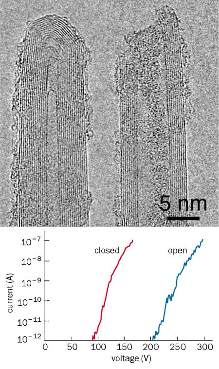
6 Field emission from nanotubes (a) Transmission electron microscope images of closed (left) and open multiwall nanotubes used in field-emission experiments. (b) Current-voltage characteristics for field emission from open and closed nanotubes. Closed nanotubes can produce significant emission currents at much lower voltages than open nanotubes (J-M Bonard et al. 1999 Appl. Phys. A69 245)
Here, we will focus on measurements of field emission from different types of nanotubes by Jean-Marc Bonard and co-workers at EPFL. To make a field-emission source with just one nanotube, individual multiwall nanotubes were mounted onto a gold tip. The nanotubes were kept in place by van der Waals forces alone (i.e. adhesive was not used). Bonard and co-workers compared the field emissions from multiwall nanotubes with open and closed ends (figure 6). Nanotubes grown in arc discharges are normally closed, but they can be opened by applying a very large electric field, or by treating them with oxygen at high temperature. Field emission occurred when a potential of a few hundred volts was applied to the gold tip. Both open and closed nanotubes were capable of emitting currents as high as 0.1 mA, which represents a tremendous current density for such a small object.
Surprisingly, closed nanotubes were much more efficient than open ones (figure 6b). This was surprising because the smaller effective curvature of the open nanotubes was expected to lead to a larger field amplification. It is now thought that other species (such as oxygen atoms) attach themselves to the free dangling bonds at the end of the nanotube, resulting in localized electron states. Since these states lie well below the Fermi energy in the nanotube, they cannot emit electrons. Localized states are also thought to form at the tips of closed nanotubes. However, these states couple to so-called p-orbitals in the nanotube and this effectively enhances the emission of electrons. This also has the advantage of narrowing the energy distribution of the emitted electrons. Electron microscopy is one application in which this effect would be very useful.
Carbon nanotubes exhibit a wealth of properties and phenomena. While many of these are understood, others remain controversial, and nanotubes are sure to remain an exciting area of condensed-matter physics for years to come. The amazing structural and electronic properties of nanotubes are not in doubt. Like any new technology, however, nanotubes will have to outperform current technology to gain a foothold in commercial markets. All these challenges will keep nanotube researchers busy for a long time to come.
Further reading
General articles
C Dekker 1999 Carbon nanotubes as molecular quantum wires Physics Today May pp22-28
M Dresselhaus et al. 1998 Carbon nanotubesPhysics World January pp33-38
Mechanical properties
M R Falvo et al. 1997 Bending and buckling of carbon nanotubes under large strain Nature 389 582-84
P Poncharal et al. 1999 Electrostatic deflections and electromechanical resonances of carbon nanotubes Science 283 1513-16
M M J Treacy, T W Ebbesen and J M Gibson 1996 Exceptionally high Young’s modulus observed for individual carbon nanotube Nature 381 678-80
E W Wong, P E Sheehan and C Lieber 1997 Nanobeam mechanics: elasticity, strength, and toughness of nanorods and nanotubes Science 277 1971-75
M-F Yu et al. 2000 Strength and breaking mechanism of multiwalled carbon nanotubes under tensile load Science 287 637-40
Electronic, magnetic and quantum properties
A Bachtold et al. 1999 Aharonov-Bohm oscillations in carbon nanotubes Nature 397 673-75
S Frank et al. 1998 Carbon nanotube quantum resistors Science 280 1744-46
C Schönenberger et al. 1999 Interaction and interference in multiwall carbon nanotubes Appl. Phys. A69 283-295
K Tsukagoshi, B W Alphenaar and H Ago 1999 Coherent transport of electron spin in a ferromagnetically contacted carbon nanotube Nature 401 572-74