Golf clubs have an intrinsic attraction to physicists. Not only is the game a relaxing sport, but designing the perfect golf club requires the modelling of some very complex interactions. Manufacturers have to take into account vibration, flexibility and rotational torque dynamics to make sure that the maximum amount of power or energy is transferred from the head of the club to the ball.
One way to minimise the effect of rotational torque is to reduce the drag produced by the club. Some inventors have altered the surface of the club by embedding circular dimples evenly across the surface to reduce drag. Others have used fine grooves to create a turbulent air boundary layer on the outer surface of the club. This air cushion reduces the drag and the rotational torque around the club head.
Patent 5700208 has taken these ideas one stage further by implementing dimples in a coordinated pattern to mimic the effect of both the grooves and the dimples.
COBE first hit both the scientific and international headlines in the early nineties when it confirmed that the cosmic background radiation followed a blackbody spectrum, and later when it detected fluctuations in the cosmic background.
COBE was switched off in 1994, but astronomers are still analyzing the data it collected. Two years ago, a French team led by Jean-Loup Puget of the Institut d’Astrophsique Spatiale in Orsay, claimed to have seen a background glow in data taken by COBE’s Diffuse Infrared Background Experiment (DIRBE). This instrument measured infrared radiation at ten different wavelengths between 1 and 240 micrometers.
Now, astronomers at the Space Telescope Science Institute have re-analyzed the COBE data and come to the same conclusion. Their analysis removed the infrared radiation produced by the solar system, by stars in our galaxy, and by dust clouds within the Milky Way.
The maps contain a uniform glow across the whole sky. Cosmologists believe that by measuring the infrared brightness at all ten wavelengths, they can put a limit on the total amount of energy released by all the stars in the universe. Michael Rowan-Robinson, an astrophysicist at Imperial College in London, believes it is an important result for astronomy. “A number of groups, including my own, have been predicting a strong far infrared background for a number of years, and this confirmed detection is very good news” he says.
The results also indicate that telescopes, such as the Hubble Space Telescope, have not observed all the light produced by distant stars. This may be because vast dust clouds have blocked the early starlight. Alternatively a early explosion of star formation could have been so far in the past that the stars cannot be visualized with existing astronomical equipment.
Carolyn S Shoemaker and her husband Eugene M Shoemaker – two of the discoverers of comet Shoemaker-Levy 9 – have won the James Craig Watson Medal for their contributions to astronomy. In the last twenty five years they have discovered over 800 asteroids and 32 comets. Sadly Eugene Shoemaker died in a car crash last year while conducting field research on impact crater research.
In a fitting tribute, his ashes were launched onboard the Lunar Prospecter spacecraft last week. When its batteries fail, the probe will crash onto the surface of the Moon. Shoemaker once said that “not going to the moon and banging on it with my own hammer has been the biggest disappointment in life”.
The NAS Award in Applied Mathematics and Numerical Analysis goes to Paul R Garabedian of New York University for his work on computational fluid dynamics.
Wayne A Hendrickson of Columbia University receives the Alexander Hollaender Award in Biophysics. Hendrickson was chosen for his contributions to macromolecular crystallography.
Finally the award for scientific reviewing goes to James R Holton, of the University of Washington, Seattle, for his reviews on the dynamical meteorology of the Earth’s stratosphere.
The awards will be presented in Washington DC on 27 April.
The new evidence is published in this week’s Nature. Two papers, one by David Gray of the University of Western Ontario, and one by Artie Hatzes of the University of Texas, Austin, describe new information that indicates a planet orbiting the star 51 Pegasi.
The planet was originally discovered by Michel Mayor and Didier Queloz of the Geneva Observatory. They studied doppler shift patterns in the star’s spectral absorption lines. Their calculations suggested the planet was approximately half Jupiter’s mass and moved in a very close orbit around the star. At the time, this small orbit made some astronomers skeptical that such an object could really exist.
Gray pointed out that the star could generate periodic oscillations producing doppler shift patterns similar to those seen by Mayor and Queloz. His new data now refutes this theory: “a planet may indeed be the best explanation for the radial-velocity results” he writes. In a connected paper Hatzes and his colleagues describe some high resolution results that are consistent with the existence of a planetary companion to 51 Pegasi.
Last week astronomers in Toronto published a paper which indicated a mechanism for Jupiter mass planets to move from outlying orbits to smaller orbits (Science279 69-72, 1998). Together the three papers increase the likelihood that doppler shifts in our neighboring stars really are generated by massive planets.
The official citation states that the awards are made “for the discovery of quantum topological and geometrical phases, specifically the Aharonov-Bohm effect, the Berry phase, and their incorporation into many fields of physics”. These fields include optics, nuclear physics, fluid physics, chemistry, molecular physics, string theory, gravitational physics, cosmology, solid-state physics, the foundations of quantum mechanics and quantum computing.
In 1959 Aharonov and the late David Bohm proposed a thought experiment in which a charged particle is directed towards a tube of magnetic flux. The particle is split quantum mechanically so that one component passes to one side, say the left, of the tube, while the other passes to the right. Although the magnetic field is zero outside the tube, the vector potential associated with the field is not zero. This led Aharonov and Bohm to predict that the two components of the electron would acquire different phases due to their interaction with the vector potential – even though the field itself was zero – and that the difference between these phases could be detected via interference. The effect was soon observed in experiments.
In 1984 Berry showed that, under certain conditions, quantum systems could acquire what is known as a geometric phase. Berry was studying quantum systems in which the Hamiltonian describing the system is slowly changed so that it eventually returns to its initial form. Berry showed that the adiabatic theorem widely used to describe such systems was incomplete. In particular he found that the system acquired a phase factor that depended on the path followed, but not on the rate at which the Hamiltonian was changed. This geometric phase factor, now known as the Berry phase, was later shown to be a generalization of the Aharonov-Bohm effect.
Aharonov currently holds joint appointments at Tel Aviv University in Israel and the University of South Carolina in the US. Berry is Royal Society Research Professor at the University of Bristol in the UK. The Prize, worth $100, 000, will be presented by the president of Israel, Ezer Weizman, in Jerusalem in May.
According to the Xinhua news agency, Russia will supply two 1, 000 megawatt nuclear reactors to Lianyungang in the eastern Jiangsu province. The reactors are expected to come on-line in 2004 and 2005.
China is seen by all the major nuclear power companies as one of the fastest growing markets in the world. Only one percent of China’s energy needs presently comes from nuclear power and over $60 billion is expected to be spent on nuclear reactors in the next fifteen years.
Russia is not the only player in the market. Recently both Canada and France have struck agreements with China to provide financing and technology for the country’s fledgling nuclear industry. Earlier this year, President Clinton authorized sales of US reactors to China.
A number of different radiation sources, such as gamma-rays and X-rays, have been used to pasteurize intact eggs. However, the high radiation dose needed to kill Salmonella and other bacteria leads to two side effects – a deterioration in the physical structure of the egg white, and a revolting smell. This means the eggs cannot be fried or poached (but they can be boiled).
Patent 5700504 describes a method to reduce the problem. Before irradiation the egg is heated to 54 – 62 Celsius for up to 45 minutes. This decreases the deterioration, and reduces the smell. Eggs packaged in sealed containers flushed with carbon dioxide, add additional protection to the egg white when undergoing this process.
Interest in the Moon was heightened with the deployment of the Defense department’s Clementine spacecraft into lunar orbit four years ago. In 1996 the Pentagon announced that water ice had been found inside craters at the southern pole. It is suspected that the ice is the remains of cometary bombardment over two billion years ago. However evidence was inconclusive. Lunar Prospector should be able to confirm or disprove the existence of water on the Moon.
The spacecraft was launched from Cape Canaveral, Florida, on an Athena II solid rocket late Tuesday night. The probe will orbit the Moon approximately 100 km above its surface.
The primary mission is expected to last one year and will generate a complete geological map of the surface using five instruments. These include: a gamma ray spectrometer for measuring the chemical composition of the lunar surface; a magnetometer for measuring the magnetic fields of the Moon, Earth, and solar wind; an alpha particle spectrometer for analyzing outgassing from the lunar interior; an electron reflectometer for measuring the Moon’s magnetic field at the lunar surface; and a neutron spectrometer to search for hydrogen. This last instrument should provide definite proof for the existence, or otherwise, of water on the suface.
Another passive experiment will measure the doppler effect – frequency changes of the spacecraft’s radio signal. This information provides data on the shape of the Moon’s gravity field. Changes in this field can indicate large mineral deposits or mass concentrations near the surface. During the extended mission, the spacecraft will drop to an altitude of 10km above the surface to improve data accuracy by a factor of 100.
Lunar Prospector is expected to go into lunar orbit shortly. Primary investigators are scheduled to start releasing data to other researchers sometime in June.
In an article published in the December 22 issue of Chemical and Engineering News, Russian scientists have spoken of their stuggle to survive. The average cost of living in Moscow is about $200 per month, but the average salary of a senior scientist is between $100 – $150 per month. Many have taken second jobs in a attempt to make ends meet.
Researchers also face a stuggle to upgrade or maintain aging equipment. State funding is now only enough to pay salaries and graduate student stipends, and no funds are available for libraries, buildings, maintence, or essential utilities. The academic’s have had to rely on private companies and international institutions for support.
Massive staff cuts have occurred at many of the institutions privatized during 1993-1995 and funding from the Defense Ministry, which funded 75 percent of all research, has completely dried up. Russia is also at the bottom of industrialized countries in terms of GDP spent on research. In yet another decline, science will receive only 2.8 percent of the 1998 budget.
In an attempt to promote their subject to a indifferent public, scientists have started taking to the streets: in October over 250 scientists picketed the Russia Parliament demanding that science funding be raised to 4% as required by law.
It is not even certain that the remaining institutes have escaped closure. Vladimir Bulgak, the vice prime minister for science and high technology, has suggested that 30% of the Russian Academy of Science institutes should be closed.
Many scientists are moving to the west. An estimated 70, 000 to 90, 000 researchers between the ages of 30-45 emigrate from Russia every year, with most scientists leaving the country shortly after graduation. More are moving out of science altogether. Nikolai Plate, secretary general for science at the Russian Academy of Sciences, is quoted as being more worried about the internal brain drain than the external.
There is however some good news; Institutes and universities have more autonomy than in the past, and there are no limitations on international activities. Some groups have even started to thrive.
Carbon nanotubes are unique nanostructures with remarkable electronic and mechanical properties. Interest from the research community first focused on their exotic electronic properties, since nanotubes can be considered as prototypes for a one-dimensional quantum wire. As other useful properties have been discovered, particularly strength, interest has grown in potential applications. Carbon nanotubes could be used, for example, in nanometre-sized electronics or to strengthen polymer materials.
An ideal nanotube can be thought of as a hexagonal network of carbon atoms that has been rolled up to make a seamless cylinder. Just a nanometre across, the cylinder can be tens of microns long, and each end is “capped” with half of a fullerene molecule. Single-wall nanotubes can be thought of as the fundamental cylindrical structure, and these form the building blocks of both multi-wall nanotubes and the ordered arrays of single-wall nanotubes called ropes. Many theoretical studies have predicted the properties of single-wall nanotubes.
1 Basics of structure A carbon nanotube is based on a two-dimensional graphene sheet, (a) The chiral vector is defined on the hexagonal lattice as Ch = nâ1 + mâ2, where â1 and â2 are unit vectors, and n and m are integers. The chiral angle, θ, is measured relative to the direction defined by â1. This diagram has been constructed for (n, m) = (4, 2), and the unit cell of this nanotube is bounded by OAB’B. To form the nanotube, imagine that this cell is rolled up so that O meets A and B meets B’, and the two ends are capped with half a fullerene molecule. Different types of carbon nanotubes have different values of n and m. (b) Zigzag nanotubes correspond to (n, 0) or (O, m) and have a chiral angle of 0°, armchair nanotubes have (n, n) and a chiral angle of 30°, while chiral nanotubes have general (n, m) values and a chiral angle of between 0° and 30°. According to the theory, nanotubes can either be metallic (green circles) or semiconducting (blue circles).
It appears that the first carbon filaments of nanometre dimensions were prepared in the 1970s by Morinobu Endo, as part of his PhD studies at the University of Orleans in France. He grew carbon fibres about 7 nm in diameter using a vapour-growth technique, but these filaments were not recognized as nanotubes and were not studied systematically. It was not until 1991, when Sumio Iijima of the NEC Laboratory in Tsukuba used high-resolution transmission electron microscopy to observe carbon nanotubes, that the field really started to take off. Researchers at the Institute of Chemical Physics in Moscow independently discovered carbon nanotubes and nanotube bundles at about the same time, but these generally had a much smaller length-to-diameter ratio. The shape of these nanotubes led the Russian researchers to call them “barrelenes”.
The discovery of fullerenes by Harold Kroto of Sussex University in the UK and Richard Smalley and co-workers at Rice University in the US stimulated researchers to explore carbon filaments further. Indeed, the realization that the ends of carbon nanotubes must be fullerene-like “caps” explained the fact that the diameter of a carbon nanotube could only be as small as a fullerene molecule.
Although Iijima’s first observations were of multi-wall nanotubes, he observed single-wall carbon nanotubes less than two years later, as did Donald Bethune and colleagues at IBM Almaden in California. In 1996 the Rice group, led by Smalley, synthesized bundles of aligned single-wall carbon nanotubes for the first time. The bundles contained many nanotubes with a narrow distribution of diameters, making it possible to perform experiments relevant to one-dimensional quantum physics. Several groups have now measured some of these remarkable properties, which seem to confirm many of the theoretical predictions.
Focus on structure
A few key studies have explored the structure of carbon nanotubes using high-resolution microscopy techniques. These experiments have confirmed that nanotubes are cylindrical structures based on the hexagonal lattice of carbon atoms that forms crystalline graphite. Three types of nanotubes are possible, called armchair, zigzag and chiral nanotubes, depending on how the two-dimensional graphene sheet is “rolled up”.
The different types are most easily explained in terms of the unit cell of a carbon nanotube – in other words, the smallest group of atoms that defines its structure (figure 1a). The so-called chiral vector of the nanotube, Ch, is defined by Ch = nâ1 + mâ2, where â1 and â2 are unit vectors in the two-dimensional hexagonal lattice, and n and m are integers. Another important parameter is the chiral angle, which is the angle between Ch and â1.
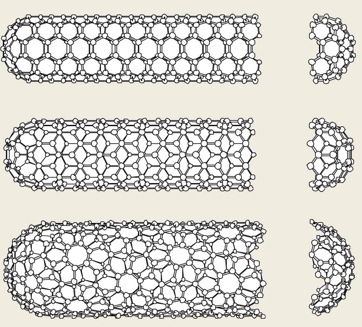
2 Models of nanotubes Nanotubes are formed by rolling up a graphene sheet into a cylinder and capping each end with half of a fullerene molecule. Shown here is a (5,5) armchair nanotube (top), a (9,0) zigzag nanotube (middle) and a (10,5) chiral nanotube. The diameter of the nanotubes depends on the values of n and m.
When the graphene sheet is rolled up to form the cylindrical part of the nanotube, the ends of the chiral vector meet each other. The chiral vector thus forms the circumference of the nanotube’s circular cross-section, and different values of n and m lead to different nanotube structures (figure 1b). Armchair nanotubes are formed when n = m and the chiral angle is 30° (figure 2). Zigzag nanotubes are formed when either n or m are zero and the chiral angle is 0°. All other nanotubes, with chiral angles intermediate between 0° and 30°, are known as chiral nanotubes.
The properties of nanotubes are determined by their diameter and chiral angle, both of which depend on n and m. The diameter, dt, is simply the length of the chiral vector divided by ¼, and we find that dt = (√3/p)ac-c(m2 + mn + n2)1/2, where ac-c is the distance between neighbouring carbon atoms in the flat sheet. In turn, the chiral angle is given by tan-1(√3n/(2m + n)).
Measurements of the nanotube diameter and the chiral angle have been made with scanning tunnelling microscopy and transmission electron microscopy. However, it remains a major challenge to determine dt and q at the same time as measuring a physical property such as resistivity. This is partly because the nanotubes are so small, and partly because the carbon atoms are in constant thermal motion. Also, the nanotubes can be damaged by the electron beam in the microscope.
Since each unit cell of a nanotube contains a number of hexagons, each of which contains two carbon atoms, the unit cell of a nanotube contains many carbon atoms. If the unit cell of a nanotube is N times larger than that of a hexagon, the unit cell of the nanotube in reciprocal space is 1/N times smaller than that of a single hexagon.
How to make nanotubes
When the Rice University group found a relatively efficient way to produce bundles of ordered single-wall nanotubes in 1996, it opened new opportunities for quantitative experimental studies on carbon nanotubes. These ordered nanotubes are prepared by the laser vaporization of a carbon target in a furnace at 1200 °C. A cobalt-nickel catalyst helps the growth of the nanotubes, presumably because it prevents the ends from being “capped” during synthesis, and about 70-90% of the carbon target can be converted to single-wall nanotubes. By using two laser pulses 50 ns apart, growth conditions can be maintained over a larger volume and for a longer time. This scheme provides more uniform vaporization and better control of the growth conditions. Flowing argon gas sweeps the nanotubes from the furnace to a water-cooled copper collector just outside of the furnace.
Catherine Journet, Patrick Bernier and colleagues at the University of Montpellier in France later developed a carbon-arc method to grow similar arrays of single-wall nanotubes. In this case, ordered nanotubes were also produced from an ionized carbon plasma, and joule heating from the discharge generated the plasma. Several other groups are now making bundles of single-wall carbon nanotubes using variants of these two methods. However, the Rice group has had the largest impact on the field, largely because it was the first to develop an efficient synthesis method and has formed many international collaborations to measure the properties of single-wall nanotubes.
In a scanning electron microscope, the nanotube material produced by either of these methods looks like a mat of carbon ropes. The ropes are between 10 and 20 nm across and up to 100 µm long. When examined in a transmission electron microscope, each rope is found to consist of a bundle of single-wall carbon nanotubes aligned along a single direction. X-ray diffraction, which views many ropes at once, also shows that the diameters of the single-wall nanotubes have a narrow distribution with a strong peak.
For the synthesis conditions used by the Rice and Montpellier groups, the diameter distribution peaked at 1.38 ± 0.02 nm, very close to the diameter of an ideal (10, 10) nanotube. X-ray diffraction measurements by John Fischer and co-workers at the University of Pennsylvania showed that bundles of single-wall nanotubes form a two-dimensional triangular lattice. The lattice constant is 1.7 nm and the tubes are separated by 0.315 nm at closest approach, which agrees with prior theoretical modelling by Jean-Christophe Charlier of the University of Louvain-la-Neuve in Belgium and co-workers.
3 Dispersion relations in nanotubes These dispersion relations show how the electronic energy in three types of nanotube varies with wavevector. Each curve corresponds to a single quantum subband. The Fermi level is at E = 0: states of lower energy are fully occupied, while higher energy states are completely empty. In an armchair (5,5) nanotube (left) and a zigzag (9,0) nanotube (middle), an infinitesimally small amount of energy is needed to excite an electron into an empty excited state, and such nanotubes are metallic. For a zigzag (10,0) nanotube (right) there is a finite band gap between the occupied and empty states, so this nanotube is a semiconductor. A small increase in diameter has a major impact on the conduction properties of carbon nanotubes.
While multi-wall carbon nanotubes do not need a catalyst for growth, single-wall nanotubes can only be grown with a catalyst. However, the detailed mechanisms responsible for growth are not yet well understood. Experiments show that the width and peak of the diameter distribution depends on the composition of the catalyst, the growth temperature and various other growth conditions. Great efforts are now being made to produce narrower diameter distributions with different mean diameters, and to gain better control of the growth process. From an applications point of view, the emphasis will be on methods that produce high yields of nanotubes at low cost, and some sort of continuous process will probably be needed to grow carbon nanotubes on a commercial scale.
Electrons in nanotubes
The unique electronic properties of carbon nanotubes are due to the quantum confinement of electrons normal to the nanotube axis. In the radial direction, electrons are confined by the monolayer thickness of the graphene sheet. Around the circumference of the nanotube, periodic boundary conditions come into play. For example, if a zigzag or armchair nanotube has 10 hexagons around its circumference, the 11th hexagonal will coincide with the first. Going around the cylinder once introduces a phase difference of 2p.
Because of this quantum confinement, electrons can only propagate along the nanotube axis, and so their wavevectors point in this direction. The resulting number of one-dimensional conduction and valence bands effectively depends on the standing waves that are set up around the circumference of the nanotube. These simple ideas can be used to calculate the dispersion relations of the one-dimensional bands, which link wavevector to energy, from the well known dispersion relation in a graphene sheet.
Noriaki Hamada and colleagues, then at the NEC Laboratory in Tsukuba, and one of us (RS) have calculated dispersion relations for small-diameter nanotubes (figure 3). These show that about one-third of small-diameter nanotubes are metallic, while the rest are semiconducting, depending on their diameter and chiral angle (figure 1b). In general, an (n, m) carbon nanotube will be metallic when n – m = 3q, where q is an integer. All armchair nanotubes are metallic, as are one-third of all possible zigzag nanotubes.
4 Energy states in metallic nanotubes The one-dimensional density of states for (8,8), (9,9), (10,10) and (11,11) armchair nanotubes show discrete peaks at the positions of the one-dimensional band maxima or minima. For these metallic nanotubes, the density of states is non-zero at E = 0. Optical transitions can occur between mirror-image spikes, such as A→B.
The density of electronic states as a function of energy has been calculated for a variety of nanotubes. As an example, consider the density of states for metallic (8, 8), (9, 9), (10, 10) and (11, 11) armchair nanotubes (figure 4). While conventional metals have a smooth density of states, these nanotubes are characterized by a number of singularities, where each peak corresponds to a single quantum subband. These singularities are important when interpreting experimental results, such as measurements obtained from scanning tunnelling spectroscopy and resonant Raman spectra, the two techniques that have contributed the most to our understanding of the one-dimensional properties of nanotubes.
Although the choice of n and m determines whether the nanotube is metallic or semiconducting, the chemical bonding between the carbon atoms is exactly the same in both cases. This surprising result is due to the very special electronic structure of a two-dimensional graphene sheet, which is a semiconductor with a zero band gap. In this case, the top of the valence band has the same energy as the bottom of the conduction band, and this energy equals the Fermi energy for one special wavevector, the so-called K-point of the two-dimensional Brillouin zone (i.e. the corner point of the hexagonal unit cell in reciprocal space). Theory shows that a nanotube becomes metallic when one of the few allowed wavevectors in the circumferential direction passes through this K-point.
As the nanotube diameter increases, more wavevectors are allowed in the circumferential direction. Since the band gap in semiconducting nanotubes is inversely proportional to the tube diameter, the band gap approaches zero at large diameters, just as for a graphene sheet. At a nanotube diameter of about 3 nm, the band gap becomes comparable to thermal energies at room temperature.
Calculations by one of us (RS) and Charlier show that concentric pairs of metal-semiconductor and semiconductor-metal nanotubes are stable. Nanometre-scale devices could therefore be based on two concentric nanotubes or the junction between nanotubes. For example, a metallic inner tube surrounded by a larger semiconducting (or insulating) nanotube would form a shielded cable at the nanometre scale. One might then envisage nanoscale electronic devices made completely from carbon that would combine the properties of metals and semiconductors, without the need for doping (see Physics World 1996 May p18).
Measurements versus theory
Experiments to test these remarkable theoretical predictions have been extremely difficult to carry out, largely because the electronic properties are expected to depend strongly on the diameter and chirality of the nanotube. Apart from the problems associated with making electronic or optical measurements on structures just a nanometre across, it is also important to gain information on the symmetry of the nanotube (i.e. its n and m values). Despite these difficulties, pioneering experimental work has confirmed the main theoretical predictions about the electronic structure of nanotubes.
Early experiments focused on multi-wall nanotubes, since high-quality single-wall nanotubes were not available in great enough quantities. To begin with, however, measurements on individual multi-wall nanotubes did not measure any one-dimensional quantum effects, largely because the diameters of the nanotubes were too large or the studies were not done at low enough temperatures.
Despite these problems, some of the early experiments on individual multi-wall nanotubes did detect a variety of novel electrical properties, including two-dimensional quantum-interference effects due to weak localization and universal-conductance fluctuations. But the results from multi-wall nanotubes are complicated by simultaneous contributions from concentric nanotubes with different diameters and chiralities. In addition, defects in the nanotubes can lead to electron scattering, and electrical contact cannot be made reliably to all of the constituent nanotubes. The conduction properties of the electrical contacts can also influence electron transport. Further experimental studies of these intriguing transport phenomena should be made on smaller diameter multi-wall nanotubes and at low temperatures, where one-dimensional quantum effects can be observed.
A key breakthrough came in 1994, when Charles Olk and Joseph Heremans of the General Motors Research Laboratory in Michigan measured the properties of individual multi-wall nanotubes using a scanning tunnelling microscope (STM). These results provided the first confirmation that some nanotubes are metallic, while others are semiconducting. Olk and Heremans also showed that the band gap for semiconducting nanotubes is proportional to 1/dt, in agreement with theoretical predictions. However, these techniques are most sensitive to the outer shell of a multi-wall nanotube, since STM probes have a relatively short spatial range. Very recent STM experiments at the Delft University of Technology in the Netherlands have clearly shown the predicted one-dimensional density of states and the difference in behaviour between metallic and semiconducting nanotubes.
Earlier this year, electron transport in an individual single-wall carbon nanotube just a nanometre across was measured for the first time by Cees Dekker and colleagues at Delft, in collaboration with the Rice group. Another group, led by Paul McEuen at the University of California at Berkeley, also working with the Rice group, has also made related measurements on a single rope of single-wall carbon nanotubes (see Physics World 1997 June p21).
Both of these studies were carried out at temperatures below 1 K and focused on the “quantum dot” aspect of single-wall carbon nanotubes. Although nanotubes are very much longer than they are wide (typically by a factor of 104), the finite length of the tubes still limits the number of allowed wavevectors along the nanotube axis. This gives rise to discrete energy states, which can be determined by measuring the conductance as a function of voltage. For a nanotube 3 µm long, the Delft group found that discrete states near the Fermi level are separated by about 0.6 meV. With the greater availability of single-wall nanotubes, we can expect that voltage-current characteristics will soon be obtained for carbon nanotubes with known n and m values. Such information could then be used to test the one-dimensional dispersion relations predicted by theory.
Since nanotubes are typically a few microns long, electrical contacts can be made by modern lithographic techniques. Single-wall carbon nanotubes thus provide a unique system for studying single-molecule transistor effects, in which an electrode close to the conducting nanotube is used to modulate the conductance.
The energy needed to add an electron to a single-wall nanotube has also been measured. Some 2.6 meV is needed to overcome the Coulomb repulsion between electrons in a nanotube 3 µm long and about 1 nm in diameter. Researchers are now beginning to study these “Coulomb-blockade” phenomena systematically in carbon nanotubes.
Recent progress in synthesizing carbon nanotubes should also stimulate experimental studies of the junction between metallic and semiconducting nanotubes, which should in turn encourage further discussions about possible electronic applications. Experimental studies on single-wall nanotubes would also test the recent predictions of one of us (RS), and of Hiroshi Ajiki and Tsuneya Ando at the University of Tokyo, about what should happen to the dispersion relations in a magnetic field.
Nanotubes in the light
Some of the most interesting one-dimensional quantum effects of carbon nanotubes have been observed in Raman spectra, which probe the lattice vibrations, or “phonons”, in a material through the inelastic scattering of light. One-dimensional dispersion relations for the phonons in nanotubes have been calculated, first by Radi Jishi of the California State University at Los Angeles using the zone-folding method, and later by Ernst Richter and co-workers at the University of Kentucky using an ab initio modelling technique. These calculations show that there are many different vibrational modes, which result from the large number of carbon atoms in the unit cell of the nanotube. In general, more phonon modes appear as the nanotube diameter and the size of the unit cell increases.
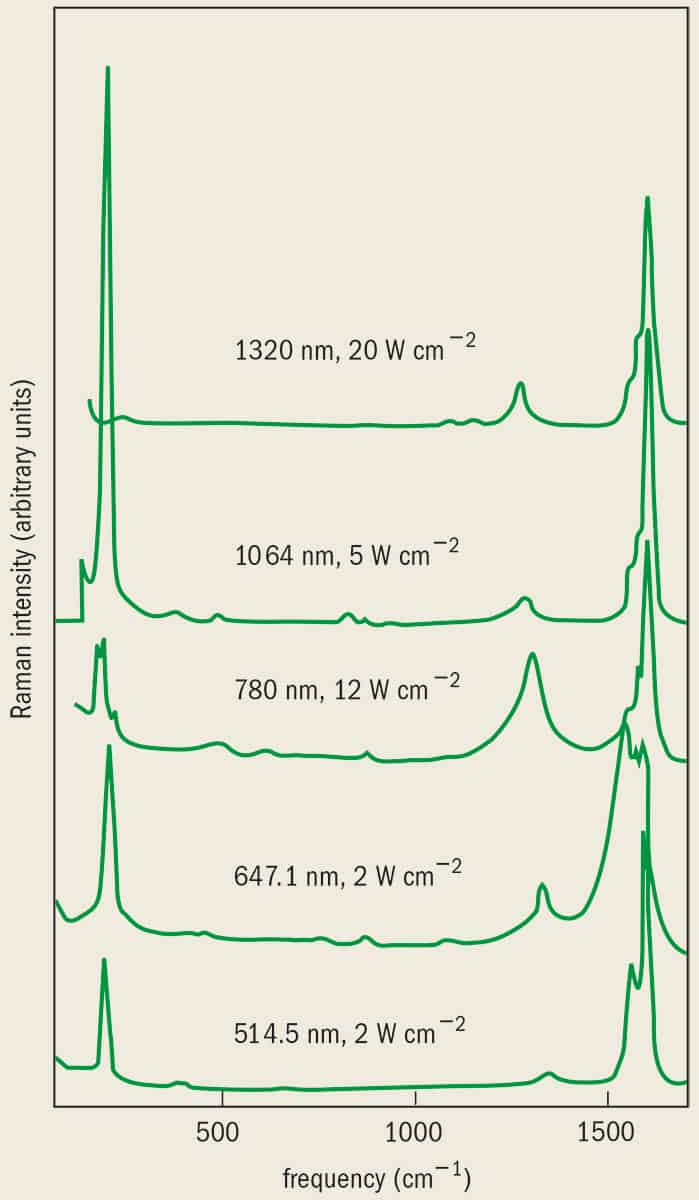
5 Light scattering from nanotubes Raman spectra for single-wall carbon nanotubes were measured at room temperature after excitation at five different laser wavelengths. A wavelength of 1320 nm corresponds to photons of energy 0.94 eV, while the other wavelengths correspond to 1.17,1.58,1.92 and 2.41 eV. The peak at a frequency of 1580 cm–1 does not depend strongly on the diameter of the tube, while the one at about 186 cm–1 does.
Of these vibrational modes, only a few can be excited by Raman scattering. The number of these Raman-active modes is independent of the nanotube diameter, which makes it possible to investigate how the frequency and oscillator strength of each mode depends on the nanotube diameter. Some modes have been found to be highly sensitive to the nanotube diameter, while others are not.
One of us (PE) and colleagues at the University of Kentucky have performed Raman-scattering experiments on ropes of single-wall carbon nanotubes grown by the Rice group, which contain a large concentration of (9, 9) and (10, 10) armchair nanotubes. These experiments exploited the resonant Raman enhancement effect, in which the frequency of the laser light matches the energy of an allowed optical transition between peaks in the density of states (figure 4). Such a resonance greatly increases the intensity of the observed Raman effect.
The Kentucky group and Bruce Chase at the Dupont Research Facility in Wilmington, Delaware, measured Raman spectra at several different laser excitation energies (figure 5). Since the energies of the electron states depend on the nanotube diameter, a change in laser frequency brings a carbon nanotube with a different diameter into resonance. Prominent in the spectra are a number of modes near a frequency of 1580 cm-1, which show only a weak dependence on nanotube diameter. There is also a strong mode at about 186 cm-1 that is highly sensitive to the nanotube diameter. This feature corresponds to a radial-breathing mode, in which all of the atoms in the nanotube are displaced outwards (or inwards) by an equal amount, so that the symmetry of the network of carbon atoms remains the same throughout the vibration. From the measured frequency of the radial-breathing mode, we can determine the diameter of the nanotube that is in resonance with the laser frequency.
Detecting these quantum effects in the Raman spectra lends strong credence to the idea that single-wall carbon nanotubes have a one-dimensional electronic and phonon structure. These experiments, together with very recent STM observations by Jeroen Wildöer and co-workers at Delft have provided the clearest confirmation to date that the electronic density of states have singularities typical of a one-dimensional system.
Strength in applications
Another exciting area of research is focused on the mechanical properties of carbon nanotubes. By analogy to graphite and carbon fibres, nanotubes are expected to be very strong and have high elastic moduli. In 1996 a group led by Thomas Ebbeson at the NEC Research Institute in Princeton, New Jersey, estimated the Young’s modulus of a carbon nanotube by measuring the vibrations of the free end of a nanotube that was clamped at the other end. Their estimates were consistent with the exceptionally high values of Young’s modulus already measured for a graphene sheet, about 1 TPa.
Single-wall carbon nanotubes are also expected to be very strong and to resist fracture under extension, just as the carbon fibres commonly used in aerospace applications. According to calculations by Jerzy Bernholc and colleagues at North Carolina State University in Raleigh, a nanotube could be elongated by several per cent before it would fracture. Unlike carbon fibres, however, single-wall nanotubes are remarkably flexible. They can be twisted, flattened and bent into small circles or around sharp bends without breaking, and severe distortions to the cross-section of nanotubes do not cause them to break (figure 6). Moreover, molecular dynamics simulations by Bernholc and colleagues indicate that in many cases the nanotube should regain its original shape when the stresses distorting it are removed.
6 Twists and turns Carbon nanotubes can be bended and twisted around sharp corners. This image, taken with a high-resolution transmission electron microscope, was produced by Morinobu Endo of Shinshu University in Japan.
Another advantage of nanotubes is their behaviour under compression. Unlike carbon fibres, which fracture easily under compression, carbon nanotubes form kink-like ridges that can relax elastically when the stress is released. As a result, nanotubes not only have the desirable properties of carbon fibres, but are also much more flexible and can be compressed without fracture. Such excellent mechanical properties could lead to applications in their own right, or in conjunction with other desirable properties.
Richard Superfine and colleagues at the University of North Carolina in Chapel Hill have shown that the mechanical properties of carbon nanotubes would make them ideal for manipulating other nanoscale structures. Advances in understanding carbon nanotubes should therefore have a major impact on the whole field of nanotechnology. Many of the applications now being considered involve multi-wall nanotubes, partly because they have been available for much longer, and partly because many of these applications do not explicitly depend on the one-dimensional quantum effects found mainly in single-wall nanotubes.
It has also been suggested that carbon nanotubes could be used in displays or for the tips of electron probes. Pulickel Ajayan and co-workers at Rensselaer Polytechnical Institute in Troy, New York, have shown that the caps of nanotubes are more chemically reactive than the cylindrical sections, and a group at the Ecole Polytechnique Fédérale Lausanne in Switzerland, then led by Walter ter Heer, has shown that the caps are efficient electron emitters. Other applications could result from the fact that carbon nanotubes can retain relatively high gas pressures within their hollow cores. Charles Lieber of Harvard University has also suggested that carbon nanotubes could act as a template for synthesizing new carbides structured on the nanoscale.
As we have seen, structures based on carbon nanotubes offer exciting possibilities for nanometre-scale electronic applications. In the same way that carbon fibres are used in composites to strengthen a structure or to enhance the electrical conductivity of the main constituent, carbon nanotubes could be combined with a host polymer (or metal) to tailor their physical properties to specific applications. Since carbon nanotubes are so small, they could be used in polymer composites that could be formed into specific shapes, or in a low-viscosity composite that could be sprayed onto a surface as a conducting paint or coating. Fundamental studies of the rheological properties of nanotube-polymer composites will be interesting from both a scientific and a practical point of view.
Intense research into carbon nanotubes is sure to continue for at least the next few years. Quantum effects and other unique features in their electronic structure will be explored further, particularly as well characterized single-wall nanotubes become more widely available. Experiments with single-wall nanotubes will also probe their lattice vibrations, as measured by Raman spectroscopy, and their mechanical properties. As we learn more about nanotubes, producing novel electronic devices and composite materials could just be the start of a variety of future applications.
This work was partially supported by the US National Science Foundation (MD, GD, PE), by the New Energy and Industrial Development Organization (NEDO) (MD, GD, RS) and by the Japanese Ministry of Education (RS).