Here at Physics World we are always on the look out for physicists with extraordinary talents outside of science. In 2023, for example we were in awe of Harvard University’s Jenny Hoffman who ran across the US in 47 days, 12 hours and 35 minutes – shattering the previous record by one week.
Now, coverage of the Winter Olympics in Italy has revealed that the Chinese freestyle skier Eileen Gu had studied physics at Stanford University. The most decorated female Olympic freestyle skier in history, US-born Gu bagged two gold medals and a silver at the 2022 Beijing games and added three silvers at Milano Cortina.
Gu has subsequently switched majors to international relations at Stanford, but we can still celebrate her as an honorary physicist.
Physics-rich event
Indeed, freestyle skiing is quite possibly the most physics-rich of all Olympic events. Athletes must consider friction, gravity and the conservation of momentum and angular momentum to perfect their skiing.
Now, I’m not suggesting that studying free-body diagrams of freestyle manoeuvres is essential for Olympic success, but I live in hope that an understanding of classical mechanics can improve one’s skiing. (I’m not sure why I believe this, because a PhD and decades of writing about physics certainly hasn’t improved my skiing!).
As well as being lauded for her prowess on the snow, Gu has found herself at the centre of an international furore regarding her choice of competing for China rather than for the US. So, international relations combined with physics seems like a very good course of study!
Article has been updated to include Gu’s third silver medal at Milano Cortina.
A new way of extracting energy from ocean waves has been proposed by a researcher in Japan. The system couples a gyroscope to an electrical generator and could be fine tuned to extract energy from a wide range of wave conditions. A prototype of the design is currently being built for testing in a wave tank. If successful, the system could be used to generate electricity onboard ships.
Ocean waves contain huge amounts of energy and humans have tried to harness this energy for centuries. But, despite the development of myriad technologies and a number of trials, the widespread commercial conversion of wave energy remains an elusive goal. One important problem is that most generation schemes only work within a narrow range of wave conditions – and the ocean can be a very messy place.
Now, Takahito Iida at the University of Osaka has proposed a new energy-harvesting technology that uses gyroscopic flywheel system that can be tuned to absorb energy efficiently over a broad range of wave frequencies.
“Wave energy devices often struggle because ocean conditions are constantly changing,” says Iida. “However, a gyroscopic system can be controlled in a way that maintains high energy absorption, even as wave frequencies vary.”
Wobbling top
At the heart of the technology is gyroscopic precession, whereby a torque on a rotating object causes the object’s axis of rotation to trace out a circle. This is familiar to anyone who has played with a spinning top, which will wobble (precess) when perturbed.
Iida’s device is called a gyroscopic wave energy converter and comprises a spinning flywheel mounted on a floating platform (see figure). On calm seas, the gyroscope’s axis of rotation points in a fixed direction thanks to the conservation of angular momentum. However, waves will cause the platform to pitch from side-to-side, exerting torques on the gyroscope and causing it to precess. It is this precession that drives a generator to deliver electrical power.
To design the system, Iida used linear wave theory to model the coupled interactions between waves, the platform, the gyroscope and the generator. This allowed him to devise a scheme for tuning the gyroscope frequency and generator parameters so that an energy conversion efficiency of 50% is achieved for a variety of wave conditions.
The effect of the generator was modelled as a spring-damper. This is a system that responds to a torque by storing and then returning some energy to the gyroscope (the spring), and removing some energy by converting it to electricity (the damper). Iida discovered that a maximum conversion of 50% occurs when the spring coefficient of the generator is adjusted such that the gyroscope’s resonant frequency matches the resonant frequency of the floating platform.
Fundamental constraint
Iida explains that 50% is the maximum efficiency that can be achieved. “This efficiency limit is a fundamental constraint in wave energy theory. What is exciting is that we now know that it can be reached across broadband frequencies, not just at a single resonant condition.”
Iida tells Physics World that a small prototype (approximately 50 cm3 in size) is being built and will be tested in a 100 m-long tank.
The next step will be the development of a system with a generating capacity of about 5 kW. Iida says that the ultimate goal is a 300 kW generator.
Iida also explains that the gyroscopic wave energy converter is designed to operate untethered to the seabed. As a result he says the system would be ideal for use as an auxiliary power system for a ship. “The target output of 300 kW is based on the assumed auxiliary power demand of a typical commercial vessel,” says Iida.
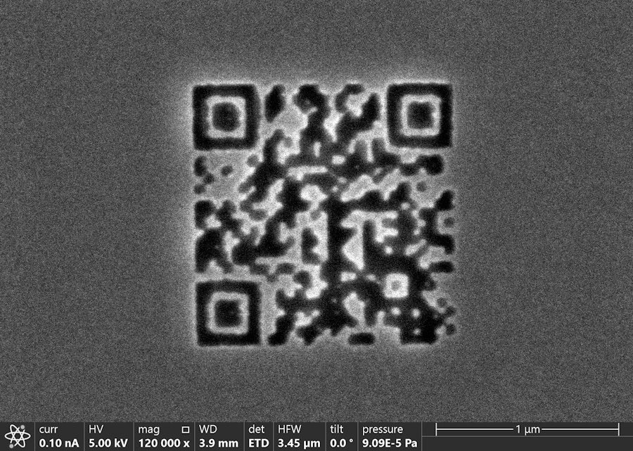
A team headed up at TU Wien in Austria has set the Guinness World Record for creating the world’s smallest QR code. Working with industry partner Cerabyte, the researchers produced a stable and repeatedly readable QR code with an area of just 1.977 µm2. When read out – using an electron microscope, as its structure is too fine to be seen with a standard optical microscope – the QR code links to a scientific webpage at TU Wien.
But this wasn’t just a ploy to get into the record books, the QR code was created as part of the team’s research into ceramic data storage materials. Unlike conventional magnetic or electronic data storage media, which degrade within decades, ceramic-based storage is designed to withstand extreme temperatures, radiation, chemical corrosion and mechanical damage.
As such, information stored in ceramic materials could endure for centuries, or even millennia. And in contrast to today’s data centres, ceramics preserve stored information without any energy input and without requiring cooling.
Invisible code The world’s smallest QR code can only be read out using an electron microscope. (Courtesy: TU Wien)
To create these ultralong-life data storage systems, the researchers use focused ion beams to mill the QR code into a thin film of chromium nitride, a durable ceramic often used to coat high-performance cutting tools. As each individual pixel is just 49 nm in size, roughly 10 times smaller than the wavelength of visible light, the code cannot be imaged using visible light. But when examined with an electron microscope, the QR code could indeed be read out reliably.
After the writing process, the entire stack of ceramic films is subjected to extreme conditions, such as high temperatures, corrosive environments and mechanical stress, to evaluate the material’s long-term durability and readout stability.
Pushing storage to its limits
Creating a “tiny QR code” was not the team’s initial goal, but emerged as a natural outcome of pushing this storage technology to its limits, says Paul Mayrhofer from TU Wien’s Institute of Materials Science and Technology.
“During a discussion with one of my PhD students, Erwin Peck, we realised that the writing procedure we had developed already produced features smaller than what had previously been reported for QR codes,” he explains. “This sparked the idea: if we can reliably write structures at that scale, why not intentionally create the smallest QR code possible?”
To claim its place in the record books, the QR code was successfully milled and read out in the presence of witnesses and its size independently verified using calibrated scanning electron microscopy at the University of Vienna. It is now officially recognized by Guinness as the world’s smallest QR code, and is roughly one third the size of the previous record holder.
Mayrhofer points out that the storage capacity of the ceramic data storage technology far surpasses that of a single QR code. “Based on current estimates, a cartridge of 100 x 100 x 20 mm with ceramic storage medium could potentially store on the order of 290 terabytes of raw data,” he says.
As well as offering this impressive raw capacity, for practical applications it’s also crucial that the ceramic storage offers high writing speed, which determines how efficiently large datasets can be stored, and low energy consumption during writing, which will influence the potential for scalability and sustainability. The researchers are currently working to optimize both of these parameters.
“Humanity has preserved information for millennia when carved in stone, yet much of today’s digital information risks being lost within decades,” project leader Alexander Kirnbauer tells Physics World. “Our long-term goal is to create an ultrastable, sustainable data storage technology capable of preserving information for extremely long times – potentially thousands to millions of years. In essence, we want to develop a form of storage that ensures the knowledge of our digital age does not disappear over time.”
Developing practical technologies for quantum information systems requires the cooperation of academic researchers, national laboratories and industry. That is the mission of the Quantum Systems Accelerator (QSA), which is based at the Lawrence Berkeley National Laboratory in the US.
The QSA’s director Bert de Jong is my guest in this episode of the Physics World Weekly podcast. His academic research focuses on computational chemistry and he explains how this led him to realise that quantum phenomena can be used to develop technologies for solving scientific problems.
In our conversation, de Jong explains why the QSA is developing a range of qubit platforms − including neutral atoms, trapped ions, and superconducting qubits – rather than focusing on a single architecture. He champions the co-development of quantum hardware and software to ensure that quantum computing is effective at solving a wide range of problems from particle physics to chemistry.
We also chat about the QSA’s strong links to industry and de Jong reveals his wish list of scientific problems that he would solve if he had access today to a powerful quantum computer.
A newly identified metallic material that conducts heat nearly three times better than copper could redefine thermal management in electronics. The material, which is known as theta-phase tantalum nitride (θ-TaN), has a thermal conductivity comparable to low-grade diamond, and its discoverers at the University of California Los Angeles (UCLA), US say it breaks a record on heat transport in metals that had held for more than 100 years.
Semiconductors and insulators mainly carry heat via vibrations, or phonons, in their crystalline lattices. A notable example is boron arsenide, a semiconductor that the UCLA researchers previously identified as also having a high thermal conductivity. Conventional metals, in contrast, mainly transport heat via the flow of electrons, which are strongly scattered by lattice vibrations.
Heat transport in θ-TaN combines aspects of both mechanisms. Although the material retains a metal-like electronic structure, study leader Yongjie Hu explains that its heat transport is phonon-dominated. Hu and his UCLA colleagues attribute this behaviour to the material’s unusual crystal structure, which features tantalum atoms interspersed with nitrogen atoms in a hexagonal pattern. Such an arrangement suppresses both electron–phonon and phonon–phonon scattering, they say.
Century-old upper limit for metallic heat transport
Materials with high thermal conductivity are vital in electronic devices because they remove excess heat that would otherwise impair the devices’ performance. Among metals, copper has long been the material of choice for thermal management thanks to its relative abundance and its thermal conductivity of around 400 Wm−1 K−1, which is higher than any other pure metal apart from silver.
Recent theoretical studies, however, had suggested that some metallic-like materials could break this record. θ-TaN, a metastable transition metal nitride, was among the most promising contenders, but it proved hard to study because high-quality samples were previously unavailable.
Highest thermal conductivity reported for a metallic material to date
Hu and colleagues overcame this problem using a flux-assisted metathesis reaction. This technique removed the need for the high pressures and temperatures required to make pure samples of the material using conventional techniques.
The team’s high-resolution structural measurements revealed that the as-synthesized θ-TaN crystals had smooth, clean surfaces and ranged in size from 10 to 100 μm. The researchers also used a variety of techniques, including electron diffraction, Raman spectroscopy, single-crystal X-ray diffraction, high-resolution transmission electron microscopy and electron energy loss spectroscopy to confirm that the samples contained single crystals.
The researchers then turned their attention to measuring the thermal conductivity of the θ-TaN crystals. They did this using an ultrafast optical pump-probe technique based on time-domain thermoreflectance, a standard approach that had already been used to measure the thermal conductivity of high-thermal-conductivity materials such as diamond, boron phosphide, boron nitride and metals.
Hu and colleagues made their measurements at temperatures between 150 and 600 K. At room temperature, the thermal conductivity of the θ-TaN crystals was 1100 Wm−1 K−1. “This represents the highest value reported for any metallic materials to date,” Hu says.
The researchers also found that the thermal conductivity remained uniformly high across an entire crystal. H says this reflects the samples’ high crystallinity, and it also confirms that the measured ultrahigh thermal conductivity originates from intrinsic lattice behaviour, in agreement with first-principles predictions.
Another interesting finding is that while θ-TaN has a metallic electronic structure, its thermal conductivity decreased with increasing temperature. This behaviour contrasts with the weak temperature dependence typically observed in conventional metals, in which heat transport is dominated by electrons and is limited by electron-phonon interactions.
Applications in technologies limited by heat
As well as cooling microelectronics, the researchers say the discovery could have applications in other technologies that are increasingly limited by heat. These include AI data centres, aerospace systems and emerging quantum platforms.
The UCLA team, which reports its work in Science, now plans to explore scalable ways of integrating θ-TaN into device-relevant platforms, including thin films and interfaces for microelectronics. They also aim to identify other candidate materials with lattice and electronic dynamics that could allow for similarly efficient heat transport.
Synthetic materials such as plastics are designed to be durable and water resistant. But the processing required to achieve these properties results in a lack of biodegradability, leading to an accumulation of plastic pollution that affects both the environment and human health. Researchers at the Institute for Bioengineering of Catalonia (IBEC) are developing a possible replacement for plastics: a novel biomaterial based on chitin, the second most abundant natural polymer on Earth.
“Every year, nature produces on the order of 1011 tonnes of chitin, roughly equivalent to more than three centuries of today’s global plastic production,” says study leader Javier G Fernández. “Chitin and [its derivative] chitosan are the ultimate natural engineering polymers. In nature, variations of this material produce stiff insect wings enabling flight, elastic joints enabling extraordinary jumping in grasshoppers, and armour-like protective exoskeletons in lobsters or clams.”
But while biomaterials provide a more environmentally friendly alternative to conventional plastics, most biological materials weaken when exposed to water. In this latest work, Fernández and first author Akshayakumar Kompa took inspiration from nature and developed a new biomaterial that increases its strength when in contact with water, while maintaining its natural biodegradability.
Metal matters
In the exoskeletons of insects and crustaceans, chitin it is secreted in a gel-like form into water and then transitions into a hard structure. Following a chance observation that removing zinc from a sandworm’s fangs caused them to soften in water, Kompa and Fernández investigated whether adding a different transition metal, nickel, to chitosan could have the opposite effect.
By mixing nickel chloride solution (at concentrations from 0.6 to 1.4 M) with dispersions of chitosan extracted from discarded shrimp shells, the researchers entrapped varying amounts of nickel within the chitosan structure. Fourier-transform infrared spectra of resulting chitosan films revealed the presence of nickel ions, which form weak hydrogen bonds with water molecules and increase the biomaterial’s capacity to bond with water.
“In our films, water molecules form reversible bridges between polymer chains through weak interactions that can rapidly break and reform under load,” Fernández explains. “That fast reconfiguration is what gives the material high strength and toughness under wet conditions: essentially a built-in, stress-activated ‘self-rearrangement’ mechanism. Nickel ions act as stabilizing anchors for these water-mediated bridges, enabling more and longer-range connections and making inter-chain connectivity more robust”.
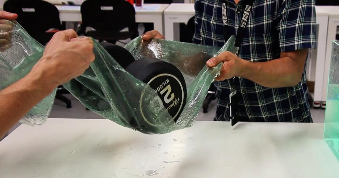
The nickel-doped chitosan samples had tensile strengths of between 30 and 40 MPa, similar to that of standard plastics. Adding low concentrations of nickel did not significantly impact the mechanical properties of the films. Concentrations of 1 M or more, however, preserved the material’s strength while increasing its toughness (the ability to stretch before breaking) – a key goal in the field of structural materials and a feature unique to biological composites.
Increased strength Testing a nickel-doped chitosan film using a 20 kg dumbbell. (Courtesy: Institute for Bioengineering of Catalonia)
Upon immersion in water, the nickel-doped films exhibited greater tensile strength, increasing from 36.12±2.21 MPa when dry to 53.01±1.68 MPa, moving into the range of higher-performance engineering plastics. In particular, samples created from an optimal 0.8 M nickel concentration almost doubled in strength when wet (and were used for the remainder of the team’s experiments).
Scaling production
The manufacturing process involves an initial immersion in water, followed by drying for 24 h and then re-wetting. During the first immersion, any nickel ions that are not incorporated into the material’s functional bridging network are released into the water, ensuring that nickel is present only where it is structurally useful.
The researchers developed a zero-waste production cycle in which this water is used as a primary component for fabricating the next object. “The expelled nickel is recovered and used to make the next batch of material, so the process operates at essentially 100% nickel utilization across batches,” says Fernández.
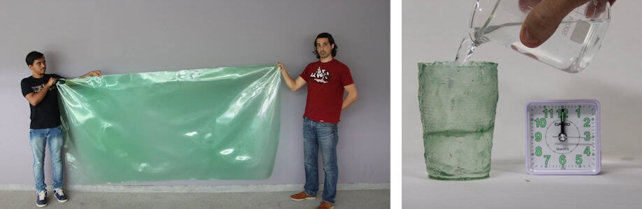
Zero waste production The team created structures including a 3 m2 nickel-doped chitosan film and a cup that can retain water as effectively as common plastics. (Courtesy: Institute for Bioengineering of Catalonia)
They used this process to produce various nickel-doped chitosan objects, including watertight containers and a 1 m2 film that could support a 20 kg weight after 24 h of water immersion. They also created a 244 x 122 cm film with similar mechanical behaviour to the smaller samples, demonstrating the potential for rapid scaling to ecologically relevant scales. A standard half-life test revealed that after approximately four months buried in garden soil, half of the material had biodegraded.
The researchers suggest that the biomaterial’s first real-world use may be in sectors such as agriculture and fishing that require strong, water-compatible and ultimately biodegradable materials, likely for packaging, coatings and other water-exposed applications. Both nickel and chitosan are already employed within biomedicine, making medicine another possible target, although any new medical product will require additional regulatory and performance validation.
The team is currently setting up a 1000 m2 lab facility in Barcelona, scheduled to open in 2028, for academia–industry collaborations in sustainable bioengineering research. Fernández suggests that we are moving towards a “biomaterial age”, defined by the ability to “control, integrate, and broadly use biomaterials and biological principles within engineering applications”.
“Over the last 20 years, working on bioinspired manufacturing, we have been able to produce the largest bioprinted objects in the world, demonstrated pathways for resource-secure and sustainable production in urban environments, and even explored how these approaches can support interplanetary colonization,” he tells Physics World. “Now we are achieving material properties that were considered out of reach by designing the material to work with its environment, rather than isolating itself from it.”
Electronics made from certain atomically thin materials can survive harsh radiation environments up to 100 times longer than traditional silicon-based devices. This finding, which comes from researchers at Fudan University in Shanghai, China, could bring significant benefits for satellites and other spacecraft, which are prone to damage from intense cosmic radiation.
Cosmic radiation consists of a mixture of heavy ions and cosmic rays, which are high-energy protons, electrons and atomic nuclei. The Earth’s magnetic field protects us from 99.9% of this ionizing radiation, and our atmosphere significantly attenuates the rest. Space-based electronics, however, have no such protection, and this radiation can damage or even destroy them.
Adding radiation shielding to spacecraft mitigates these harmful effects, but the extra weight and power consumption increases the spacecraft’s costs. “This conflicts with the requirements of future spacecraft, which call for lightweight and cost-effective architectures,” says team leader Peng Zhou, a physicist in Fudan’s College of Integrated Circuits and Micro-Nano Electronics. “Implementing radiation tolerant electronic circuits is therefore an important challenge and if we can find materials that are intrinsically robust to this radiation, we could incorporate these directly into the design of onboard electronic circuits.”
Promising transition-metal dichalcogenides
Previous research had suggested that 2D materials might fit the bill, with transistors based on transition-metal dichalcogenides appearing particularly promising. Within this family of materials, 2D molybdenum disulphide (MoS2) proved especially robust to irradiation-induced defects, and Zhou points out that its electrical, mechanical and thermal properties are also highly attractive for space applications.
The studies that revealed these advantages were, however, largely limited to simulations and ground-based experiments. This meant they were unable to fully replicate the complex and dynamic radiation fields such circuits would encounter under real space conditions.
Better than NMOS transistors
In their work, Zhou and colleagues set out to fill this gap. After growing monolayer 2D MoS2 using chemical vapour deposition, they used this material to fabricate field-effect transistors. They then exposed these transistors to 10 Mrad of gamma-ray irradiation and looked for changes to their structure using several techniques, including cross-sectional transmission electron microscopy (TEM) imaging and corresponding energy-dispersive spectroscopy (EDS) mapping.
These measurements indicated that the 2D MoS2 in the transistors was about 0.7 nm thick (typical for a monolayer structure) and showed no obvious signs of defects or damage. Subsequent Raman characterization on five sites within the MoS2 film confirmed the devices’ structural integrity.
The researchers then turned their attention to the transistors’ electrical properties. They found that even after irradiation, the transistors’ on-off ratios remained ultra-high, at about 108. They note that this is considerably better than a similarly-sized Si N-channel metal–oxide–semiconductor (NMOS) transistors fabricated through a CMOS process, for which the on-off ratio decreased by a factor of more than 4000 after the same 10 Mrad irradiation.
The team also found that MoS2 system consumes only about 49.9 mW per channel, making its power requirement at least five times lower than the NMOS one. This is important owing to the strict energy limitations and stringent power budgets of spacecraft, Zhou says.
Surviving the space environment
In their final experiment, the researchers tested their MoS2 structures on a spacecraft orbiting at an altitude of 517 km, similar to the low-Earth orbit of many communication satellites. These tests showed that the bit-error rate in data transmitted from the structures remained below 10-8 even after nine months of operation, which Zhou says indicates significant radiation and long-term stability. Indeed, based on test data, electronic devices made from these 2D materials could operate for 271 years in geosynchronous orbit – 100 times longer than conventional silicon electronics.
“The discovery of intrinsic radiation tolerance in atomically thin 2D materials, and the successful on-orbit validation of the atomic-layer semiconductor-based spaceborne radio-frequency communication system have opened a uniquely promising pathway for space electronics leveraging 2D materials,” Zhou says. “And their exceptionally long operational lifetimes and ultra-low power consumption establishes the unique competitiveness of 2D electronic systems in frontier space missions, such as deep-space exploration, high-Earth-orbit satellites and even interplanetary communications.”
The researchers are now working to optimize these structures by employing advanced fabrication processes and circuit designs. Their goal is to improve certain key performance parameters of spaceborne radio-frequency chips employed in inter-satellite and satellite-to-ground communications. “We also plan to develop an atomic-layer semiconductor-based radiation-tolerant computing platform, providing core technological support for future orbital data centres, highly autonomous satellites and deep-space probes,” Zhou tells Physics World.
In this work, the researchers theoretically explore how quantum materials can transition continuously from one ordered state to another, for example, from a magnetic phase to a phase with crystalline or orientational order. Traditionally, such order‑to‑order transitions were thought to require fractionalisation, where particles effectively split into exotic components. Here, the team identifies a new route that avoids this complexity entirely.
Their mechanism relies on two renormalisation‑group fixed points in the system colliding and annihilating, which reshapes the flow of the system and removes the usual disordered phase. A separate critical fixed point, unaffected by this collision, then becomes the new quantum critical point linking the two ordered phases. This allows for a continuous, seamless transition without invoking fractionalised quasiparticles.
The authors show that this behaviour could occur in several real or realistic systems, including rare‑earth pyrochlore iridates, kagome quantum magnets, quantum impurity models and even certain versions of quantum chromodynamics. A striking prediction of the mechanism is a strong asymmetry in energy scales on the two sides of the transition, such as a much lower critical temperature and a smaller order parameter where the order emerges from fixed‑point annihilation.
This work reveals a previously unrecognised kind of quantum phase transition, expands the landscape beyond the usual Landau-Ginzburg-Wilson framework, which is the standard theory for phase transitions, and offers new ways to understand and test the behaviour of complex quantum systems.
Unlike crystals, whose atoms arrange themselves in tidy, repeating patterns, glass is a non‑equilibrium material. A glass is formed when a liquid is cooled so quickly that its atoms never settle into a regular pattern, instead forming a disordered, unstructured arrangement.
In this process, as temperature decreases, atoms move more and more slowly. Near a certain temperature –theglass transition temperature – the atoms move so slowly that the material effectively stops behaving like a liquid and becomes a glass.
This isn’t a sharp, well‑defined transition like water turning to ice. Instead, it’s a gradual slowdown: the structure appears solid long before the atoms would theoretically cease to rearrange.
This slowdown can be extrapolated and be used to predict the temperature at which the material’s internal rearrangement would take infinitely long. This hypothetical point is known as the ideal glass transition. It cannot be reached in practice, but it provides an important reference for understanding how glasses behave.
Despite years of research, it’s still not clear exactly how glass properties depend on how it was made – how fast it was cooled, how long it aged, or how it was mechanically disturbed. Each preparation route seems to give slightly different behaviour.
For decades, scientists have struggled to find a single measure that captures all these effects. How do you describe, in one number, how disordered a glass is?
Recent research has emerged that provides a compelling answer: a configurational distance metric. This is a way of measuring how far the internal structure of a piece of glass is from a well‑defined reference state.
When the researchers used this metric, they could neatly collapse data from many different experiments onto a single curve. In other words, they found a single physical parameter controlling the behaviour.
This worked across a wide range of conditions: glasses cooled at different rates, allowed to age for different times, or tested under different strengths and durations of mechanical probing.
As long as the experiments were conducted above the ideal glass transition temperature, the metric provided a unified description of how the material dissipates energy.
This insight is significant. It suggests that even though glass never fully reaches equilibrium, its behaviour is still governed by how close it is to this idealised transition point. In other words, the concept of the kinetic ideal glass transition isn’t just theoretical, it leaves a measurable imprint on real materials.
This research offers a powerful new way to understand and predict the mechanical behaviour of glasses in everyday technologies, from smartphone screens to industrial coatings.
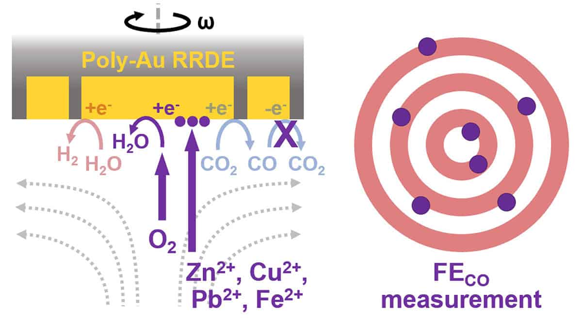
Electrochemical CO2 reduction converts CO2 to higher-value products using an electrocatalyst and could pave the way for electrification of the chemical industry. A key challenge for CO2 reduction is its poor selectivity (faradaic efficiency) due to competition with the hydrogen evolution reaction in aqueous electrolytes. Rotating ring-disk electrode (RRDE) experiments have become a popular method to quantify faradaic efficiencies, especially for gold electrocatalysts. However, such measurements suffer from poor inter-laboratory reproducibility. This work identifies the causes of variability in RRDE selectivity measurements by comparing protocols with different electrochemical methods, reagent purities, and glassware cleaning procedures. Electroplating of electrolyte impurities onto the disk and ring surfaces were identified as major contributors to electrocatalyst deactivation. These results highlight the need for standardized and cross-laboratory validation of CO2RR selectivity measurements using RRDE. Researchers implementing this technique for CO2RR selectivity measurements need to be cognizant of electrode deactivation and its potential impacts on faradaic efficiencies and overall conclusions of their work.
Maria Kelly is a Jill Hruby Postdoctoral Fellow at Sandia National Laboratories. She earned her PhD in Professor Wilson Smith’s research group at the University of Colorado Boulder and the National Renewable Energy Laboratory. Her doctoral work focused on characterization of carbon dioxide conversion interfaces using analytical electrochemical and in situ scanning probe methods. Her research interests broadly encompass advancing experimental measurement techniques to investigate the near-electrode environment during electrochemical reactions.