A new study on the mechanical stability of bonds between the spike protein on the SARS-CoV-2 virus and its receptors on human cells during infection has revealed differences in the binding stability of viral variants such as Omicron and Delta. The finding, from researchers in the Netherlands, Germany and the US, could help explain why some variants spread more quickly than others.
SARS-CoV-2, the virus responsible for COVID-19, contains four structural proteins: envelope (E); membrane (M); nucleocapsid (N); and spike (S). The M, E and S proteins are vital for assembling and forming the virus’ outermost layer, including the mechanisms by which the virus enters host cells. The N protein, meanwhile, encapsulates the virus’ genetic information.
Magnetic tweezers technique
In the new work, a team led by physicist Jan Lipfert of Utrecht University in the Netherlands used a highly sensitive technique called magnetic tweezers to study the biomechanical properties of chemical bonds in the SARS-CoV-2 virus under conditions that mimic those of the human respiratory tract. Their assay uses a protein construct that combines the receptor-binding domain of the virus (essentially the tip of the spike protein) and the extracellular domain known as ACE2 (the virus’ cellular receptor and a key entry point into human cells). These two components are connected via a flexible peptide linker.
“In addition, our construct features peptide tags to attach it with one end to a surface and with one end to a small magnetic bead,” explains Lipfert. “Using this construct, we can apply precisely calibrated forces to the interface of the virus protein bound to its cellular receptor.”
Since the two binding partners are connected with a linker, they can rebind after the bond breaks, he adds. “This allows us to study the interactions over and over again, at different forces.”
Stronger binding
The researchers found that while all the major SARS-CoV-2 variants (including Alpha, Beta, Gamma, Delta and Omicron) have a higher binding affinity to human cells than the original strain, the binding of the Alpha variant is especially mechanically stable. This could explain why it spread so quickly in late 2020 and early 2021, in populations with little or no prior immunity to the virus.
They also found, however, that the more recent Delta and Omicron variants do not necessarily bind more strongly than the others, meaning that other processes must be considered when predicting which variants might become more prevalent.
Lipfert and colleagues say that their initial idea, early in the pandemic, was to use force spectroscopy to study how the coronavirus binds to cells. “In February and March 2020, we were wondering how our expertise in biophysics might help fight the global pandemic,” Lipfert explains. “While were we working on developing the first assay, which was detailed in a preprint in autumn 2020 and finally published in PNAS, the different variants-of-concern emerged and spread around the world. This naturally led us to ask the question as to whether our assay could also be used to probe for differences between the variants.”
“We would also like to use our method to test predicted and observed new variants of the coronavirus,” Lipfert tells Physics World. “In addition, we believe our approach could be very valuable for understanding host-pathogen interactions more generally.”
Hair cools the head in hot weather, while keeping the scalp warm in the cold – according to a new study of how human hair interacts with infrared radiation. The research was done by scientists in South Korea, who hope their work will inspire the development of new textiles with optimized radiative properties.
Despite accounting for only 2% of a typical human’s mass, the head consumes about 20% of the energy burned by the body’s metabolism. The head’s skin temperature can be over 2°C warmer than elsewhere in the body, so good thermal management is therefore crucial – particularly when the Sun is beating down onto the scalp.
Hair is an evolutionary adaptation to protect the head from both damaging solar radiation and cold. At first sight it might seem that the price of this protection is a limit on the body’s ability to keep the head cool on hot days by radiating heat from the scalp.
Radiative properties
Now, however, the materials scientist Gunwoo Kim and colleagues at the Korea Institute of Industrial Technology in Yeongcheon have challenged this view by investigating the radiative properties of hair. As well as gaining insights into hair’s infrared properties, the team has also studied how they affect the heating and cooling of the scalp a various ambient temperatures.
Hair comprises three radial layers of which the middle layer (the cortex) is by far the thickest. The cortex consists of intertwined bundles mainly made of the protein keratin and air pockets that gives hair its mechanical properties such as its strength. The outer layer is called the cuticle, which comprises multiple layers of thin, flat cells overlapping like roof tiles.
The principal absorber of solar radiation in hair (and skin) is the pigment melanin. This is polymer of an organic amino acid with rings that absorb a broad spectrum of radiation between the near-infrared and the ultraviolet.
Hair models
Kim’s group investigated how the physical and chemical properties of hair combine to affect its absorptivity (which is the same thing is its emissivity according to Kirchoff’s law of thermal radiation), reflectivity, and transmission at different wavelengths. This was done using mathematical models and by doing experiments on black hair (which is rich in melanin) obtained from a local salon.
They found that the hair samples absorbed around 80% of incident light at the infrared wavelength of 1 μm, which is the maximum intensity wavelength in solar radiance. The team also studied hair samples in which the melanin had been removed by bleaching. In these samples, the absorbance was around 40%. The team repeated its measurements for infrared light at 10 μm, which is not a significant component of sunlight. After bleaching melanin they found that the absorptivity (and emissivity) at this wavelength remained around 90%. This is because the absorbance of radiation at this wavelength is largely due to chemical bonds in molecules other than melanin – molecules such as keratin.
Next, the researchers soaked the hairs in water. They found that the proportion of solar-wavelength radiation absorbed dropped significantly, whereas the proportion of radiation absorbed at 10 μm was relatively unaffected.
Scattering pores
“Human hair has pores that are almost 1 μm,” says Kim, “Those pores are very specific for scattering in the near-infrared region…To completely block solar radiation we need a large length of hair: but if we scatter the radiation inside the material we can completely block the radiation without needing such a volume of material.”
Filling the pores and edges with water had prevented the abrupt changes in refractive index and thereby reduced the scattering necessary to increase the path length of near-infrared radiation in the hair. At longer wavelengths likely to be emitted by the human body as heat, however, the waves were not scattered but absorbed and re-emitted. The team chose to study 10 μm radiation because it is in the centre of an atmospheric “transparency window”. “We call this phenomenon radiative cooling because we can emit this radiation easily to space,” says Kim.
The researchers then conducted field trials. They found that, on a cold day, a sample of synthetic skin covered with hair ended up being warmer than the bare skin. On a warm day, however, hair-covered synthetic skin remained cooler. The researchers are now looking to develop bio-inspired textiles based on the principles outlined in a paper describing the research in Proceedings of the National Academy of Sciences.
Luis Ruiz Pestana is an expert in the modelling of nanostructured materials at the University of Miami in the US. He told Physics World that these results are both impressive and puzzling.
“The really unique thing is not that you absorb UV light, but that hair seems to be really good at emitting in the infrared,” he says; “So basically you get that UV light, you absorb it, and you release it in the infrared spectrum.”
However, he is perplexed by the cold temperature behaviour, for which the researchers provide data but little explanation: “I didn’t understand at all [how] the architecture of hair allows the infrared to remain trapped between the skin and the atmosphere,” he says “So first part very clear, second part not so clear.”
Scientists at the Universities of Vienna, Austria and Helsinki, Finland have captured the first direct images of clusters of room-temperature noble gas atoms by confining them in a “sandwich” made from two layers of graphene. Taken using a transmission electron microscope, the images could aid fundamental condensed-matter physics research and might have applications in quantum technology.
Led by physicist Jani Kotakoski, the team obtained the images while studying how radiation modifies the properties of graphene (a sheet of carbon just one atom thick) and other two-dimensional materials held together by weak van der Waals interactions. The scientists noticed that when they used noble gas ions to irradiate a sample of multilayer graphene, the ions could become trapped between two sheets of the material. For this to happen, the energy of the irradiating ions had to be just right: fast enough to pass through the first sheet, but not the second.
“We succeeded in doing this by implanting the noble gas ions into the multi-layered structures,” explains team member Manuel Längle, who began working on this project during his master’s thesis in late 2017. “If we find the implanted ions in a five-layer but not a two-layer sample, we know that the energy is too high.”
In their work, which is published in NatureMaterials, the researchers studied krypton and xenon ion clusters using scanning transmission electron microscopy (STEM). They found that for krypton-irradiated samples, successful implantation between two graphene layers occurred at 60 eV. For xenon-irradiated samples, the “sweet spot” was between 55 eV and 65 eV.
Densely-packed two-dimensional nanoclusters
Because noble gases are mostly inert and seldom form chemical bonds, the atoms can move about freely within their graphene sandwich. In certain regions, however, two or more atoms can come together and form regular, densely-packed two-dimensional nanoclusters. These nanoclusters make an excellent testbed for studies of very weakly-interacting systems.
The researchers found that clusters of xenon made up of up to 100 atoms behave like solid systems but that krypton clusters containing as few as 16 atoms sometimes show fluid-like behaviour. Though they do not yet understand why, they say the finding could open a new field of study focused on encapsulated van der Waal materials.
According to Längle and Kotakoski, applications for these structures are difficult to predict at present. However, since noble gases are routinely employed in light sources and lasers, they might have some future use in quantum information technology.
Looking forward, the Vienna-Helsinki team now plans to repeat the experiments at different temperatures and pressures. “We also plan to study mixtures of gases and look into different two-dimensional materials like hexagonal boron nitride (sometimes called ‘graphene’s cousin’) or multi-layered structures,” Längle tells Physics World.
Across all state schools in England, Black ethnic groups are among the most under-represented at physics A-level. With so few Black students opting to study physics beyond the age of 16, it should come as no surprise that Black people make up barely 1.5% of UK undergraduate physics students. This extreme under-representation can also be seen at the pinnacle of the field, where among the 825 physics professors in the UK, there are incredibly few of Black heritage.
The Blackett Lab Family is a collective of UK-based Black physicists who aim to diversify perceptions of physics and promote Black representation at all levels. Our organization, which was founded in 2020 by a close-knit group of Black physics students, alumni and staff from Imperial College London, has since grown to encompass Black physicists across the country.
One of our key objectives is to increase the number of Black UK-based students doing physics or physics-related courses or schemes. That’s why in July 2023 we ran a three-day physics experience for students of Black heritage in years 11 and 12 (ages 15 to 17). It aimed to shed light on what studying physics at university involves, to promote the value of physics to society, to strengthen the students’ physics identities and to show the benefits of diversity in physics.
Some 32 students based in London took part in Representing Physics 2023, which was launched in partnership with the Ogden Trust, Imperial College London, the National Physical Laboratory (NPL) and the Institute of Physics (IOP), which publishes Physics World. On the first day, the students were given a full taster of the undergraduate experience at Imperial. They attended, for example, lectures on topics such as special and general relativity, quantum physics and nanophotonics.
We also wanted the students to get a taste of lab work, which is a key part of the undergraduate experience. Unfortunately, schools often have limited resources and time to develop the skills to conduct experiments, which can end up dissuading students from pursuing physics at university. We therefore gave students a tour of Imperial’s undergraduate labs and led them through experiments in electromagnetism. We ended the day discussing the options available to them, providing tips on how to write strong applications, and giving advice for academic success at A-level.
The second day of the programme was hosted at the NPL, where our students visited labs, met scientists and engineers, and were shown the value of physics to society. They saw, for example, the lab from which time signals are distributed to the whole of the UK. These tangible examples of how the work of physicists benefits people’s lives are invaluable for students who often don’t fully appreciate how physics helps wider society. Members of the Blackett Lab Family who work in areas such as finance, law and medicine also met the students, telling them about their careers and how they use the skills from their physics degrees.
We need the physics community to play a greater role in supporting initiatives like ours
The final day – hosted at the IOP – saw a variety of interactive workshops to help the students recognize and strengthen their “physics identity”. Research carried out by the American Institute of Physics has shown that physics identity – essentially how you see yourself in physics – is critical when it comes to minoritized students succeeding in physics. The students also shared personal experiences that they felt had either threatened or affirmed their physics identities, and brainstormed solutions to strengthen their identity and to empower themselves.
Given that we often draw strength and guidance from role models, it was crucial that students on the programme learn about great physicists who look like them, who have similar backgrounds and who they can look up to. With relatively few Black physicists in the mainstream, the students took part in an interactive research activity in which they discovered and shared examples of trailblazing Black physicists such as Clifford Johnson at the University of Southern California.
We believe that it is important to get buy-in from parents, guardians and carers to support their child’s choice of pursuing physics, and to demonstrate to the students that they will be supported throughout their physics journey. So we invited parents, carers, guardians and siblings, along with our project partners and supporters, to a ceremony to celebrate the completion of the programme.
While the students enjoyed the course – one even saying it was the best three days of their life – there is still much to do. If every student in this tiny cohort went on to study physics at university, the population of Black physics undergraduates would increase by over 10%, but this would only tilt the balance of representation slightly. For each student who attended the programme, there are thousands more across the rest of the UK who would have greatly benefited from an experience like this. We barely scratched the surface.
Society will also greatly benefit from many more young people from different backgrounds becoming enthusiastic about physics, so we need the physics community to play a greater role in supporting initiatives like ours. To adapt an old saying, it takes a community to raise a physicist.
Those who have taken up running in the new year will know that buying new shoes can be a daunting experience. The right running shoes can shave valuable seconds off your personal best, but with so many options, it’s easy to get intimidated before you’ve taken a single step.
But now researchers from the Massachusetts Institute of Technology (MIT) have developed a model that can predict the most efficient shoe for an individual based on their gait.
Running shoes are designed with varying amounts of stiffness and springiness in the sole, to cushion the joints and store energy. But because everyone runs differently, the shoe that works for one athlete won’t be as effective for another.
The researchers, led by Anette Hosoi, built a mechanical model of a runner’s foot that incorporates their height, weight and leg length, as well as the mechanical properties of different shoe soles. They used this to find the shoe that optimizes each runner’s efficiency.
The researchers hope that one day, customers will be able to have a personalized shoe 3D printed, based on a video of their running gait. This would be welcome news for runners; the ability to get an optimized performance without trying on dozens of styles would leave them plenty of time to train for their next race.
Physics World produces two podcasts and much of the recording is done in North Bristol – in my home office and in Andrew Glester’s Cosmic Shed. Unfortunately, we are on an approach for Bristol Airport, with aeroplanes from Ireland flying over our heads before turning over Bath to approach the airport from the east. Despite me having double-glazed windows and a well insulated loft and walls, the occasional aeroplane noise gets onto a recording.
So I was very pleased to hear that researchers at the Swiss Federal Laboratories for Materials Science and Technology (EMPA) have come up with a way to evaluate the noise of passenger aircraft of the future. They are focusing on blended wing body (BWB) aircraft, which have fuselages that merge seamlessly into their wings. This should result in less air resistance and lower fuel consumption. What is more, these aeroplanes will have their engines mounted above the fuselage, which should deflect much of the sound up into the sky, making it quieter on the ground.
But how can aeronautical engineers ensure that this design will please podcasters and others lovers of silence? Normally, complex computer simulations are done to estimate the sound from a particular design. But the human perception of noise can be a tricky thing to understand. To get a more realistic understanding of how a new aircraft will be perceived on the ground, the team subjected real people to simulated aircraft noise in a process called auralization.
This was done at EMPA’s AuraLab, where loudspeakers were arranged in a room to recreate the sounds associated with aircraft take-off and landing. The subjects listened to the sounds made by today’s aeroplanes and to the simulated sounds of future BWB aircraft. The listeners were asked to rate how annoying the sounds were on a scale from zero to 10. The study revealed that BWB aircraft are 4.3 units less annoying than conventional aircraft. That’s great news for Bristol podcasters.
Researchers in China and the US have created a functional semiconductor made from graphene, a feat that they describe as a first. By expanding on existing fabrication techniques, Walter de Heer and colleagues at Tianjin University and the Georgia Institute of Technology have created a develop a bandgap in the 2D material, while retaining graphene’s robust and easily tuneable properties.
Silicon is the backbone of modern semiconductor electronics. However, the latest silicon-based technologies are being stretched to their limits by our relentless demand for higher computing speeds, lower power consumption, and more compact devices.
For two decades now, researchers have explored the possibility that graphene could provide a practical alternative to silicon. First isolated in 2004, graphene is a sheet of carbon just one atom thick. Since then, researchers have found that graphene has a number of properties that could make it very useful for electronic devices. These include high electron mobility; a strong, lightweight, highly compact structure; and excellent heat dissipation.
One major drawback
However, graphene has one major drawback. Unlike conventional semiconductors, graphene lacks an intrinsic electron bandgap. This is an energy barrier that electrons must overcome to conduct electricity. It is the bandgap that allows electronic switches (transistors) to be made from semiconductors.
“A long-standing problem in graphene electronics is that graphene didn’t have the right bandgap, and couldn’t switch on and off at the correct ratio,” explains co-author Lei Ma, who co-founded the Tianjin International Center for Nanoparticles and Nanosystems with de Heer. “Over the years, many have tried to address this with a variety of methods.”
Previous studies have tried to engineer appropriate bandgaps using techniques such as quantum confinement and the chemical modification of pure graphene. So far, however, these approaches have resulted in very little success.
“We had to learn how to treat [graphene], how to make it better and better, and finally how to measure its properties,” de Heer explains. “That took a very, very long time.”
Spontaneous growth
In their latest research, the researchers have shown for the first time how the bandgap semiconductor “epigraphene” can been grow spontaneously on the surfaces of silicon carbide crystals.
Previous research had revealed that at high temperatures, silicon sublimates from the surfaces of these crystals, leaving behind carbon-rich layers. These layers recrystallise into multi-layered epigraphene, which has limited semiconducting properties.
Expanding on this technique, de Heer and Ma’s team have developed a new annealing method, in which they carefully controlled the sample temperature and the rate of epigraphene formation. They created a robust graphene layer that grows in macroscopic, atomically-flat terraces. What is more, the graphene atoms are aligned with the lattice of the silicon carbide substrate.
Useful bandgap
By making careful measurements, the team showed that this layer is an excellent 2D semiconductor. It has the useful bandgap that has eluded researchers for decades, along with high electron mobility.
“We now have an extremely robust graphene semiconductor with 10 times the mobility of silicon, and which also has unique properties not available in silicon,” de Heer enthuses. He compares electron mobility in silicon to driving on a gravel road, whereas the epigraphene is like an electron freeway. “It’s more efficient, it doesn’t heat up as much, and it allows for higher speeds so that the electrons can move faster,” explains de Heer.
On top of this performance, the team also showed that their epigraphene can be doped with a wide range of atoms and molecules to fine-tune its electronic and magnetic properties. The material can also be nanopatterned to further enhance its performance further – nanopatterning is very difficult to do with graphene grown on other substrates.
De Heer, Ma and their colleagues hope that their technique could pave the way for an entirely new approach to semiconductor manufacturing, and may ultimately be a crucial first step towards a new generation of graphene-based electronics.
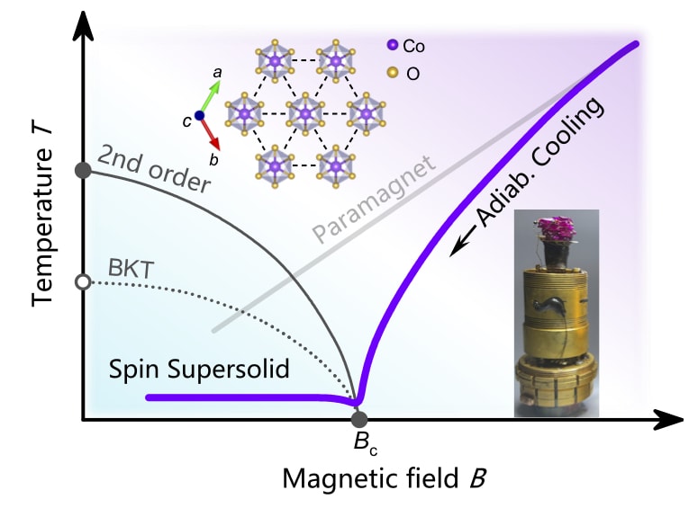
The figure illustrates the adiabatic cooling process of a spin supersolid, as compared to paramagnetic cooling, highlighting the unique features of spin supersolid cooling. The triangular lattice structure and experimental devices (with NBCP compounds) for adiabatic magnetocaloric measurements are also included in the insets. (Courtesy: W Li)
Researchers in China, France and Australia have found new evidence for an exotic quantum state of matter called a spin supersolid. The discovery, made in an antiferromagnetic material with a triangular atomic lattice structure, represents a breakthrough in fundamental physics and might also aid the development of new cooling techniques that do not require liquid helium, since the material also shows a giant magnetocaloric effect.
As their name implies, supersolids are materials that flow without friction (like a superfluid) even though their component particles are arranged in a crystalline lattice (like a solid). As such, these materials break two continuous symmetries: translational invariance, due to the crystalline order; and gauge symmetry, due to the material’s frictionless flow.
Theorists predicted in the 1960s that supersolids should exist in quantum solids with so-called mobile bosonic vacancies – that is, gaps left behind as atoms with integer spin values move through the crystalline lattice. Beginning in the 1980s, experimental research focused on hints that supersolidity might occur in superfluid helium-4. In 2004, physicists at Pennsylvania State University in the US reported evidence for supersolidity in this material. However, further investigation by the same researchers revealed that they were mistaken, and their observations could be explained in other ways.
More recent experiments have shown that dipolar quantum gases elongated in one direction can undergo a phase transition from a regular Bose-Einstein condensate (BEC) to a state with supersolid properties. Atoms in dipolar gases have large magnetic moments and it is the interactions between them that give rise to supersolidity in these systems.
Layers of evidence
Researchers led by Gang Su at the University of Chinese Academy of Sciences (CAS) in Beijing now say they have found the quantum magnetic analogue of a supersolid in a recently synthesized antiferromagnet with the chemical formula Na2BaCo(PO4)2. This compound, known as NBCP, also displays a giant magnetocaloric effect, meaning that it heats up and cools down dramatically when an external magnetic field is applied and removed.
Further confirmation came from microscopic evidence they gained by conducting neutron diffraction experiments on high-quality samples of NBCP at the Institut Laue-Langevin in France and the Australian Nuclear Science and Technology Organisation. “The diffraction peaks revealed in-plane three-sublattice order, solid order and incommensurability in the out-of-plane direction,” says Su. “The latter can be related to the existence of gapless Goldstone modes (a form of symmetry breaking in bosons) and therefore supports the existence of spin superfluidity in the compound.”
A new quantum state of matter and a new cooling mechanism
The CAS team chose to study NBCP because it exhibits strong low-energy spin fluctuations, indicating a possible quantum spin liquid state. It is also an antiferromagnet, meaning that unlike conventional ferromagnets, which have parallel electron spins, its electron spins tend to align antiparallel to each other. This anti-alignment leads to strong interactions among the spins.
After one of the team’s members suggested a spin supersolid might exist in NBCP, Li and Gang asked their experimentalist colleagues Xiang, Jin and Sun if it was possible to look for new quantum spin states in the compound. “They did and observed the new quantum state of matter, the spin supersolid,” Li recalls.
As well as revealing a new quantum state of matter, the discovery could also lead to new helium-free sub-Kelvin cooling methods. These are highly sought after for materials science, quantum technology and space applications, among others, Li tells Physics World.
Li explains that there are currently two main ways to cool materials to few-Kelvin temperatures. The first is to use helium, which becomes a liquid at temperatures below 4.15 K. The second is to exploit the magnetocaloric effect, in which certain materials change temperature under the influence of an applied magnetic field. Both these techniques have their drawbacks: helium is scarce and therefore expensive, while the special class of compounds used for magnetocaloric cooling (known as hydrated paramagnetic salts) have low magnetic entropy density, poor chemical stability and low thermal conductivity. However, Li claims that the giant magnetocaloric effect in the newly-discovered spin supersolid could “effectively overcome these drawbacks” by exploiting collective spin excitations at low energies.
Looking for other spin supersolids
The researchers are now trying to obtain additional dynamical evidence for spin supersolidity in NBCP. To this end, Jin says they are performing inelastic neutron scattering measurements to investigate the Goldstone modes associated with the spin superfluid order. They also plan to conduct polarized neutron diffraction experiments to further strengthen their findings.
Finally, the team is investigating other triangular lattice compounds in an effort to identify additional spin supersolid states or other exotic spin states. “By doing so, we hope to better understand the underlying physical phenomena that give rise to these intriguing quantum phases of matter,” Su says.
Network leader Celia Merzbacher is executive director of QED-C, an industry-driven consortium managed by SRI International. With a diverse membership representing industry, academia, government and other stakeholders, QED-C is seeking to accelerate quantum R&D, technology innovation and commercial opportunities. (Courtesy: QED-C)
Why is it important for the US and other countries to have a national strategy for quantum science and technology?
Quantum sensing, quantum networking and quantum computing technologies hold significant promise for improving national security, but also for their long-term economic and societal impacts. However, the field is still at a relatively early stage in terms of technology evolution. There’s a clear requirement for advances in fundamental science, an activity supported by government funding in the main. It’s also worth noting that quantum is what I call a “multi-type” endeavour. It’s multidisciplinary, multiagency (in terms of government support), multisector and multinational.As such, progress will be accelerated through strategic, cross-cutting and coordinated investments in a broad research portfolio.
How should countries balance their national security requirements with the need for international collaboration and global supply chains in quantum technology?
It’s understandable that national interests should play a role in controlling the flow of information in certain sensitive quantum use-cases – though, ultimately, any restrictions need to be implemented carefully and in partnership between like-minded countries. Right now, it feels premature to be overly restrictive. There’s a broad understanding of the need for open sharing of information, R&D opportunities and science/engineering talent to encourage multidisciplinary collaboration between centres of excellence all over the world.
How well positioned is the current US effort in quantum science and technology?
Looked at from an input perspective, the US is faring well, with government investment in quantum R&D for 2022 running at around $900m – and compared with an aggregate per-annum global spend on quantum across government and private sector estimated at approximately $30bn. In terms of outputs as well, the US is shaping up competitively, registering the largest numbers of highly cited, high-impact scientific publications along with China.
Is there a danger of too much hype damaging the reputation of the quantum industry?
This is a key question and one that crops up often. There’s certainly a lot of excitement and interest around the quantum sector, with growing levels of public and private-sector investment. Here at QED-C, we don’t see evidence of what might be called a “bubble” – just researchers and companies within the emerging supply chain reporting steady progress on their development roadmaps while addressing a lot of tough technology and engineering problems along the way. In fact, organizations like QED-C have a significant role to play here in managing expectations. Chiefly, that means sharing credible, evidence-based data and metrics on progress so that diverse stakeholders – policy-makers, funding agencies, the investment community and industry – have a granular understanding of the state-of-the-art and where quantum technology is heading.
There’s an acknowledged shortage of skilled workers in the quantum workforce worldwide. What skills are needed to bridge the gap?
There’s a misconception that workers need to have a PhD – preferably in physics – to enter this field. That’s absolutely not the case. Manufacturers and developers within the early-stage quantum supply chain are desperate for scientists, engineers and technicians – especially those with experience in a related field – for example, cryogenics, test and measurement, data science or circuit design. What’s more, with targeted training and staff development, it’s possible for mid-career professionals in related disciplines to pivot into a career in the quantum industry (see “Quantum technicians: scaling the talent pipeline”, below).
One thing is clear: the quantum sector is brimming with opportunity for ambitious individuals, with a range of skills needed within hardware companies, software companies and, ultimately, the end-users of quantum technologies in key verticals like pharma, finance and healthcare. We also need commercially minded technical sales people who understand how to fuel the nascent market for quantum applications. In this way, the quantum industry offers all sorts of pathways for talented scientists and engineers to evolve from mainstream technical roles into business development activities if they choose.
Quantum technicians: scaling the talent pipeline for industry
While efforts are underway to prepare students at the undergraduate, masters and PhD level for quantum engineering and scientist roles, there are few associate degree and specialist vocational education programmes geared specifically towards the training of “quantum technicians”. That’s the main take-away from Guide to Building a Quantum Technician Workforce, a new study from QED-C, a consortium of US and international stakeholders that aims to fast-track growth across the quantum industry supply chain.
Quantum technicians fulfil many key functions in quantum technology companies, including system and component fabrication, device assembly, characterization, testing, operation and maintenance. What’s more, notes the report, demand for skilled technicians “is expected to grow as the industry continues its rapid development”, with a pressing need to scale this section of the workforce in the near term.
A range of specialist domain knowledge and skills are commonly required for quantum technician roles – including experience with vacuum, cryogenic and optical systems, as well as programming and soft skills. Current hiring strategies often focus on recruiting candidates from adjacent technology sectors – microelectronics, semiconductor manufacturing and photonics among them – with in-house shadowing programmes to provide on-the-job training for new staff.
The QED-C report argues, however, for a “more coordinated approach specifically geared toward filling the quantum workforce pipeline” and, in turn, to increase productivity and commercial opportunities, especially within smaller companies.
Recommendations in the QED-C study include: defining the types of quantum technician roles and investing in marketing to build awareness about career trajectories; mapping of existing training programmes versus the knowledge, skills and abilities that quantum technicians need; and creating local partnerships between higher education, industry and the US National Laboratory system. The report also calls for the establishment of an accreditation programme for quantum technology curricula and extra cash for institutions focused on quantum training and education rather than research.
“Manufacturing of quantum systems has not yet scaled to high-volume production,” the report concludes. “As such, many assume that demand for quantum technicians is low or non-existent. This is a common misconception – in fact, quantum technician roles are highly relevant in the experimental and prototype stages.”
Guide to Building a Quantum Technician Workforce: Reskilling and Upskilling Recommendations to Prepare a Workforce of Quantum Technicians is available on an exclusive basis to members of QED-C.
QED-C was originally launched as a US initiative but has since opened its membership to organizations from 36 like-minded countries. What’s driven this shift?
Quantum R&D and technology innovation is happening on a global scale and certainly the US, at this time, does not have the sole leadership position or an enormous head-start. We recognized from the outset – along with our federal government sponsors – that international partnerships would ultimately be fundamental to the success of the QED-C mission. Equally, our members are looking at a global opportunity when it comes to markets, customers, technology partners and even investors. Helping our members succeed along those coordinates is what we try to do every day at QED-C.
Quantum pathways The quantum industry is brimming with diverse career opportunities, with a range of skillsets needed across hardware companies, software companies and, ultimately, the commercial end-users of quantum technologies. (Courtesy: Oxford Instruments NanoScience)
How should industry and government approach R&D on quantum computing given that it’s unclear which platform technologies – superconducting circuits, ion traps, photonic processors or the like – will prove commercially viable?
For government, the focus is on precompetitive basic and applied research. That means prioritizing foundational hardware and software technologies, underpinned by theoretical understanding, experimental systems, device design and fabrication – and pushing along all of these research pathways simultaneously. On the industry side, meanwhile, companies across the supply chain need to progress as quickly as possible from the R&D lab towards sustainable revenues and long-run commercial applications.
Another area that needs to be strengthened is engagement with the end-users of quantum computing in all sorts of diverse industries – from quantitative finance and insurance to medicine, telecoms, advanced materials and the rest. Over time, there will be many more “quantum takers” than “quantum makers” and all those takers need to be setting up pathfinder teams now to figure out how their respective industries will be disrupted by quantum technologies.
SBQuantum is a Canadian company that spun-out of Quebec’s University of Sherbrooke in 2017. It has developed a magnetometer that uses a superposition of quantum states to enhance its sensitivity to magnetic fields.
In this episode of the Physics World Weekly podcast, the company’s co-founder and CEO David Roy-Guay explains how the technology works and why an SBQuantum magnetometer will be launched into space as part of a multimillion-dollar competition to advance how we measure Earth’s magnetic field.
He also talks about more down-to-earth uses of the firm’s sensors in mineral exploration, navigation and security scanning.
The Japanese Space Agency, JAXA, has today announced a possible explanation for why its lunar lander is unable to generate power from its solar panels – the craft landed upside down.
While the Smart Lander for Investigating Moon (SLIM) successfully landed softly on the Moon on 20 January, engineers soon discovered that the craft was unable to generate power. It was then put in safe mode until further investigations were carried out. Today, JAXA released an image taken by a small lunar rover, ejected by the craft before it landed, which shows SLIM on its nose.
SLIM was launched on 7 September 2023 from the Tanegashima Space Center on the island of Tanegashima aboard a H-IIA Launch Vehicle. It took off alongside the X-ray Imaging and Spectroscopy Mission.
One of SLIM’s main objectives is to demonstrate high-precision “vision-based” landing to put the craft down within 100 m of the target site. This is compared to typical target lunar-landing sites that can stretch for several kilometres.
To do so, SLIM has an onboard laser-range finder, a camera and a radar. They combined to measure the altitude, imaged the lunar surface, as well as measured the altitude and speed of the craft as it descended towards the surface.
JAXA says that just before landing, SLIM lost thrust from one of the two main engines. Yet the craft still managed to land about 55 m east of the original landing site, with the craft touching down under 10 m of the landing site chosen by the craft’s real-time navigation system. “It is reasonable to mention that the technology demonstration of pinpoint landing…has been achieved,” a JAXA statement says.
Nose dive
Shortly before landing, SLIM released two small demonstrator lunar rovers. A small baseball-sized robot dubbed Lunar Excursion Vehicle-2 (LEV-2) as well as LEV-1, a lunar rover with a mass of 2.1 kg, which moves via a hopping mechanism.
JAXA says that LEV-1 was able to move on the lunar surface, but was unable to send images. The rover has now completed its activities and is in standby mode.
LEV-2, however, managed to take an image of SLIM and transmit it to Earth via LEV-1. The picture, released today, shows SLIM upside down on its nose. JAXA also released an image of the lunar surface taken by SLIM’s multi-band camera.
JAXA says that as a result of this orientation, SLIM’s solar panels are facing west, suggesting that power generation could be possible as “sunlight illumination improves over time”. The space agency says that it will now continue to “acquire further technical and scientific data” from the craft.
As a result of the soft landing, Japan became the fifth nation to successfully land a craft on the Moon, following the US, Soviet Union, China and India.