Soft and stretchable strain sensors are invaluable for use in wearable electronics such as motion tracking devices and physiological monitoring systems. Currently, however, the trade-off between sensitivity and sensing range is a major challenge. Strain sensors that are capable of detecting small deformations cannot be stretched very far, while those that can be stretched to greater lengths are typically not very sensitive.
When monitoring human physiology and motion, skin strain ranges from below 1% to over 50%. As such, separate sensors are typically used to detect subtle strains (such as those associated with blood pulse and respiration) and large strains (such as bending of body parts). But for monitoring certain diseases, use of a single device would be preferable. In Parkinson’s disease, for example, sensors must be sensitive enough to monitor small tremors while maintaining a large enough range to measure joint movements.
What’s really needed is a single sensor that can be attached to different parts of the body and can accurately measure the full range of strains on human skin. With this goal in mind, a team at North Carolina State University has developed a soft stretchable resistive strain sensor that offers high sensitivity, large sensing range and high robustness.
“The new sensor we’ve developed is both sensitive and capable of withstanding significant deformation,” explains corresponding author Yong Zhu in a press statement. “An additional feature is that the sensor is highly robust even when overstrained, meaning it is unlikely to break when the applied strain accidently exceeds the sensing range.”
The sensor, described in ACS Applied Materials & Interfaces, measures strain by measuring changes in electrical resistance. The device is made from a silver nanowire network embedded in the elastic polymer poly(dimethylsiloxane), with a series of mechanical cuts in its top surface, alternating from either side.
When the sensor is stretched, the cuts pull open. This forces the electrical signal to transition from a uniform current flow across the closed cracks to travelling further along the zigzag conducting path defined by the open cracks. Thus the resistance increases under applied strain. The opening up of the cuts also allows the device to withstand substantial deformation without reaching its breaking point. “This feature – the patterned cuts – is what enables a greater range of deformation without sacrificing sensitivity,” says first author Shuang Wu.
The team performed experiments and finite element analysis to assess the effects of slit depth, length and pitch on sensor performance. The optimized device exhibited a large gauge factor (the ratio of relative change in electrical resistance to mechanical strain) of 290.1 with a sensing range of more than 22%. It was also robust to overstrain and 1000 repeated loading cycles.
Building devices
To demonstrate some potential applications of their new strain sensor, Zhu, Wu and colleagues integrated it into wearable health monitoring systems that measure vastly different levels of motion.
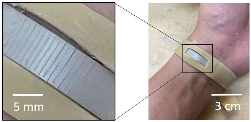
Personal health monitor The sensor is integrated with a rubber wristband to enable blood pressure monitoring. (Courtesy: Shuang Wu, NC State University)
First, they employed the sensor to monitor blood pressure, which requires extremely high sensitivity. Using a rubber band to secure the sensor, they placed it on a volunteer’s wrist to detect the pulse wave – one of the smallest strain signals on human skin.
When the blood pumps through the vein, the sensor ends remain fixed in place by the band while the centre is stretched, opening up the cracks on its top surface.
The researchers showed that this set-up could capture the pulse wave from the radial artery on the wrist. By placing another strain sensor on the brachial artery higher up on the arm and recording a second pulse wave simultaneously, they could measure the averaged pulse wave velocity, enabling calculation of blood pressure.
Measuring back strain The researchers created a wearable device for monitoring motion in a person’s back. (Courtesy: Shuang Wu, NC State University)
In the next example, the sensor was used to monitor large strains on the lower back during motion, which has utility for physical therapy. Here, the researchers integrated the sensor with a stretchable athletic tape and attached two sensors in parallel along the spine on a volunteer’s lower back. They also attached a Bluetooth board onto the back to collect and transmit the sensing signals.
Starting from a sitting straight position, the subject performed a series of movements while the sensor monitored lower back strains. When leaning forward, both sensors responded with resistance increases. While leaning forward and tilted sideways, the resistance of the sensor on the corresponding side remained near constant while the sensor on the opposite side showed substantially increased resistance.
Finally, to demonstrate the sensor’s use in human–machine interfaces, the researchers created a soft 3D touch sensor that tracks both normal and shear stresses and can be used to control a video game. They also integrated a strain sensor on the fingertip of a glove that was then used to grasp a glass of water, demonstrating its potential for tactile sensing for robotics applications.
The team is now exploring the application of the strain sensor for biomedical and sports applications. “Biomedical applications include monitoring movement patterns during rehabilitation of stroke patients,” Zhu tells Physics World. “We are also working on scalable manufacturing of the sensors.”
The 2022 Nobel Prize for Physics recognized pioneering experiments by Alain Aspect, John Clauser and Anton Zeilinger that for the first time demonstrated the potential of quantum systems for processing information. Several decades later, scientists and engineers in both industry and academia are building on these achievements to create functioning quantum computers that offer a tantalizing glimpse of their potential to tackle complex problems across a range of applications.
While the progress to date has been impressive, much more work is needed to create quantum computers that can outperform their classical counterparts. Today’s small-scale quantum processors are now pushing the number of qubits towards the 100–1000 range, but they are affected by noise and errors that limit their computational capabilities. Scaling up the technology to achieve a broad quantum advantage will take scientific ingenuity and engineering know-how across many different disciplines, as well as close collaboration between the academic and commercial sectors.
In the UK that collaboration has been driven through the National Quantum Technologies Programme (NQTP), a £1bn initiative that since 2014 has supported technology hubs in quantum sensing, imaging, communications and computing. “We have a rich ecosystem that is working together to push the scaling up of quantum computers to deliver useful applications,” says Elham Kashefi, professor of quantum computing at the University of Edinburgh and a CNRS director of research at the Sorbonne University in Paris.
Kashefi has just been appointed chief scientist of the UK’s National Quantum Computing Centre (NQCC), a facility launched in 2020 as a flagship programme of the NQTP. The NQCC aims to accelerate the delivery of quantum computing in the UK by partnering with research groups and the commercial sector to address scaling challenges.
“Part of my role with the NQCC will be to bring together application developers and end users to push forward the development of useful devices,” says Kashefi. “We are now at the stage where the requirements of the algorithms can influence the design of the hardware, allowing us to close the gap between the desired use-case and the emerging machine.”
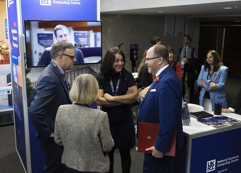
Quantum future Professor Elham Kashefi (middle) has just been appointed chief scientist of the NQCC. Kashefi is pictured here talking to science minister George Freeman (right) and NQCC director Michael Cuthbert (left) at the UK’s National Quantum Technologies Showcase in November 2022. (Courtesy: NQCC)
With a background in computer science, Kashefi has long been an advocate for the role that software and algorithms can play in developing quantum solutions. She co-ordinated the software research programme within the Quantum Computing and Simulation (QCS) Hub, a consortium of UK universities supported by the NQTP that focusses on the critical scientific challenges for quantum computing. The hub has been the launchpad for a number of start-up companies championing different hardware and software solutions, and now works with the NQCC to grow the UK quantum computing ecosystem by translating research strengths into innovative technologies.
As part of her new role, Kashefi will work with the NQCC to establish a quantum software laboratory at the University of Edinburgh, a core initiative that will further extend the national footprint of the NQCC’s programme. “The scalability challenge we are now facing with the physical qubits is a problem that computer science and applications software can help to solve,” she says. “We can optimize the requirements for the qubits by co-developing the software and control systems to address the needs of the application.”
Such co-development demands a multidisciplinary approach that combines knowledge of quantum hardware and information processing with the expertise of mathematicians and computer scientists who understand how to tackle complex computational problems.
“Connecting with the wealth of knowledge we have in classical computer science will enable us to optimize system architectures and control systems, as well as protocols for error mitigation and correction, to obtain the best result from the hardware platforms,” says Kashefi. “As an example, people working in high-performance computing have spent a lot of time figuring out how to solve optimization problems, and their input will help to accelerate the development of quantum solutions that deliver a computational advantage.”
One promising avenue is the development of hybrid approaches that combine emerging quantum devices with classical computing infrastructure. As an example, the NQCC is a partner in the QuPharma collaboration, a £6.8m project that aims to radically reduce the time needed to run molecular simulations for drugs discovery.
Led by hardware developer SEEQC UK and involving the German pharmaceutical giant Merck KgaA, the project aims to combine SEEQC’s quantum processor with a classical supercomputer to create a more powerful platform for drug design. “We need to understand the pain points in industry to enable us to translate them into research problems that quantum computing might be able to solve,” points out Kashefi.
Such collaborative projects draw on the scientific expertise harboured within the UK’s academic sector, which has nurtured world-class research in quantum theory, software and algorithms as well as experimental work investigating all the leading qubit architectures.
“As someone who is focused on applications and verification, I have been thrilled to have access to qubit platforms ranging from superconducting circuits and trapped ions through to photonics and silicon-based devices,” says Kashefi. “When we write the code we need to be aware of the capabilities and limitations of each qubit platform, since some applications may be more suited to the noise model or connectivity offered by a particular hardware solution.”
The emerging quantum industry also benefits from the strength of the science base within the UK, with many quantum start-ups maintaining close links with their former research groups to advance the technology and accelerate their development programmes.
“The academic sector acts as an ideas factory,” says David Lucas, the principal investigator of the QCS Hub and co-leader of the trapped-ion quantum-computing group at the University of Oxford. “Scaling up the technology is an engineering challenge that extends beyond the capabilities of a single university research department.” Indeed, one key role for the NQCC is to provide the infrastructure and facilitate the collaboration that will be needed to address these engineering challenges.
That synergy between industry and academia has been particularly effective in the development of the Maxwell platform, a commercial neutral-atom quantum-computing system demonstrated by M Squared, a developer of photonics and quantum technologies, at the UK’s National Quantum Technologies Showcase in November 2022. The current version of the system can support 100 qubits, and M Squared CEO Graeme Malcolm says there is a clear route to scaling the technology to 400 qubits and beyond.
“To create Maxwell we formed a strategic partnership with the University of Strathclyde, which has provided our company with access to world-class breakthrough physics,” says Malcolm. “It has been great to have a such a strong university department right on our doorstep that we can lean into for specialist expertise, while we have been able to bring the engineering capability needed to develop a reliable product.”
Maxwell is based on a neutral-atom qubit architecture perfected by Jonathan Pritchard and his research team at Strathclyde. The experimental platform, which relies on M Squared’s core laser technology to manipulate energy transitions in ultracold atoms, was developed through an EPSRC Prosperity Partnership called SQuAre.
“We worked closely with the photonics engineers at M Squared to optimize the performance of the lasers, and in some cases to design new devices tailored to the specific atomic processes we need,” says Pritchard. Meanwhile, the development of the commercial system was enabled by the DISCOVERY programme, a £10 million project co-ordinated by M Squared and supported by Innovate UK’s Quantum Technologies Challenge programme to address the technology barriers to commercial quantum computing.
One of the next steps for the collaboration will be to work with Andrew Daley, an expert in quantum simulation and computing at the University of Strathclyde, to develop quantum algorithms that demonstrate the capability of the platform. In 2021 a research team led by Harvard University in the US showed that a neutral-atom system composed of 256 qubits could be used to simulate and observe the quantum behaviour of many-body systems, and earlier this year the team used a 289-qubit version to demonstrate a pathway to quantum advantage for a specific class of analogue quantum algorithms.
“The system we have developed with the University of Strathclyde is competitive with the best neutral-atom quantum computers in the world,” says Malcolm. “Now we want to put some of those algorithms onto the hardware we have demonstrated and establish partnerships to see where it can offer value for real-world challenges.”
That need to put in place robust benchmarking and certification protocols is another important priority for Kashefi and the NQCC. Within her own research programme Kashefi has focused on developing tools for verification and testing, which she believes will help to fast-track the development of the most promising technologies.
“When different devices emerge we need to know how to evaluate them and how to compare their performance to other platforms,” she says. “A reliable testing framework provides crucial feedback that will allow us to transition more quickly to a new regime.”
In 2021 the NQCC commissioned Riverlane, a specialist in quantum algorithms and software, to develop a benchmarking suite to enable performance comparisons across different types of quantum processors. A consortium led by the National Physical Laboratory is also investigating key metrics for quantum computing, with a view towards developing open standards to underpin international technology development. “The NQCC is not trying to push any particular hardware solution, but being able to benchmark different platforms will be really useful for stimulating our own development programme as well as the wider ecosystem,” says Kashefi.
Such benchmarking will also make it possible to understand where quantum solutions offer a genuine advantage over classical computing architectures. “Quantum computing is an amazing and revolutionary technology, but ultimately it is just another computational tool,” continues Kashefi. “Proper benchmarking will enable us to understand which tasks are best suited to a classical computer, and which can be enhanced by a quantum solution.”
Cherenkov imaging enables real-time visualization of radiation beams on a patient’s body and provides a means to evaluate the accuracy of radiotherapy delivery. Researchers in China have now developed a way to improve the quality of Cherenkov images using a flexible, non-toxic sheet of carbon quantum dots (cQDs) attached to the patient.
Cherenkov light is produced when charged particles travel at a speed greater than the phase velocity of light in tissue. The signal intensity is proportional to the delivered radiation dose, revealing the precise dose that’s delivered during treatment. The optical imaging technique offers high spatial resolution, high sensitivity and fast imaging speed compared with conventional methods of radiation dose measurement.
The intensity of Cherenkov emission is low, however, and the emitted photons are scattered and absorbed by tissue. Because of this, standard charge-coupled device (CCD) cameras have difficulty collecting the signal. Instead, more expensive intensified CMOS/CCD cameras are being used.
The cQDs have absorption spectra that overlap with the Cherenkov emission spectra; they then emit luminescence at longer wavelengths. The cQD sheeting, developed and tested at the Department of Nuclear Science and Technology of Nanjing University of Aeronautics and Astronautics, can therefore be used to shift the Cherenkov emission to match the optimal wavelength of a CCD camera’s sensitive detection region.
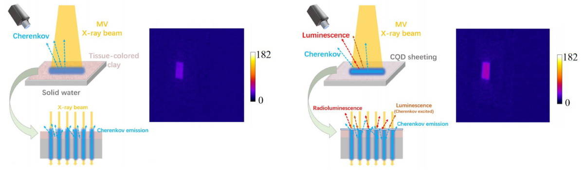
With the cQD sheeting in place, the optical emission is composed of Cherenkov photons generated in the superficial surface of the tissue, fluorescence excited by the Cherenkov photons, and the radioluminescence generated in the cQDs. This increases the total optical signal and improves the image quality and signal-to-noise ratio (SNR) of the acquired images.
Principal investigator Changran Geng and colleagues created the cQD sheeting using a solution of 10 nm-diameter cQDs and UV-curable adhesive. This mixture was spin-coated onto a substrate coated with plastic sheeting and solidified with a UV lamp. The plastic substrate ensures that the scintillation material does not directly contact the skin.
The resulting cQD sheeting had a thickness of 222±5 µm and a diameter of 15 cm, and was flexible enough to conform to the patient’s surface. The team note that the cQD sheeting is almost transparent and does not block the Cherenkov emission from tissues.
Reporting their findings in Medical Physics, the researchers initially tested the cQD sheeting on a solid water slab covered with a 2 mm layer of light coloured skin-toned clay to mimic the optical properties of skin. They evaluated the relationship between optical intensity and delivered dose using cQD concentrations of 0, 0.05 and 0.1 mg/ml, delivered doses of 100–500 MU, and 6 and 10 MV beams. They observed a linear relationship between optical intensity and dose for both 6 and 10 MV photons. Adding the cQD sheeting more than doubled the SNR in both cases.
Enhancing emission Schematic of luminescence emission and single-frame image of the luminescence from a solid water sample without (left) and with (right) the cQD sheeting. (Courtesy: Med. Phys. 10.1002/mp.16121)
The team then examined the performance of the cQD sheeting on an anthropomorphic phantom using different radiotherapy materials and various ambient light sources. Light emission from the surface of the various materials was over 60% higher with cQD sheeting than without. Specifically, the average optical intensity increased by about 69.25%, 63.72% and 61.78% when adding cQD sheeting to bolus, mask sample, and a combination of bolus and mask, respectively. The corresponding SNRs improved by about 62.78%, 56.77% and 68.80%.
Under ambient light from a red LED, optical images with a SNR of greater than 5 could be obtained through the sheeting. Adding a band-pass filter increased the SNR by about 98.85%.
“Through a combination of cQD sheeting and corresponding filter, the light intensity and SNR of optical images can be increased significantly,” the researchers write. “This sheds new light on the promotion of the clinical application of optical imaging to visualize the beam in radiotherapy with a more rapid and less expensive image acquisition process.”
Geng tells Physics World that the team is actively continuing its research in many ways. One example is investigating Cherenkov imaging for use with electron beam radiotherapy of keloids, benign fibrous lesions arising from an abnormal healing response.
“Some studies have indicated that post-operative electron beam radiotherapy can reduce the rates of keloid recurrence,” Geng explains. “However, inaccurate deliveries are commonly associated with the variation of electron beam parameters, as well as patient’s setup uncertainties or respiratory movements. These can lead to insufficient or excessive dose at the mismatched adjacent fields, potentially causing tissue damage to normal skin or keloid recurrence. We are trying to use Cherenkov imaging technology with cQD sheeting to measure matching of adjacent radiation fields delivered during keloid electron radiotherapy in real-time.”
This episode features an interview with the scientists Michelle Bell and Scott Goetz, who are editors-in-chief of two new environmental journals from IOP Publishing.
Bell is a professor of environmental health at Yale University and has helped launched the journal Environmental Research: Health. She talks about her research on how the greening of urban landscapes and other environmental factors affect human health.
Goetz heads the Global Earth Observation and Dynamics of Ecosystems lab at Northern Arizona University and has helped launch the journal Environmental Research: Ecology. He talks about how Earth observation satellites are shedding light on how climate change is affecting ecosystems such as taiga (boreal forest).
Also in this podcast, the science writer Laura Hiscott looks at a recent study that suggests that innovation in science and technology is waning.
China’s Young Thousand Talents (YTT) programme has succeeded in encouraging high-calibre, early-career Chinese scientists to return home after stints abroad. That is according to an analysis of the programme, which was set up in 2010 to entice leading scientists under 40 to work in China. The study also found that the YTT has boosted the productivity of those scientists who return to China – although very few non-Chinese researchers have taken advantage of the initiative (Science10.1126/science.abq1218).
The YTT targets science, technology, engineering and mathematics (STEM) scholars working overseas by offering them generous income subsidies and start-up grants to relocate to China. To examine whether the approach has worked, a team led by applied mathematician Dongbo Shi from Shanghai Jiao Tong University in China analysed the productivity of 339 Chinese scientists from the YTT’s first four cohorts before and after they came home.
The authors found that the returning scientists were among the most productive early-career researchers, ranking in the top 10th to 15th percentile for productivity when comparing them with scientists in the US who have Chinese surnames. Once settled in China, however, the returnees’ productivity was found to be 27% higher than overseas scientists with Chinese surnames.
The returnee scientists were found to produce fewer first-authored papers than their peers. However, they published significantly more papers in which they are named as the last author – a marker of who is the principal investigator of the work.
The authors suggest this is because YTT researchers are more likely to be running their own research groups than their overseas peers who had stayed outside of China.
Room for improvement
The authors claim that the productivity gains seen by returning scientists is linked to a greater access to funding as well as the ability to create larger research teams when they return to China. The researchers also say that their results show the potential of talent programmes to attract scientists and improve a nation’s research productivity.
The difficulty of attracting scientists who are more established, however, suggests there is still room for improvement in the YTT programme, the team says. Although open to any nationality, few non-Chinese researchers have taken advantage of the initiative.
The researchers also note that the initiative only uses a small proportion – less than 0.5% – of China’s academic research and development budget, so given its success, they advise that the programme could be scaled up. “As China continues to invest in higher education and academic talent, we can expect more Western-trained Chinese students to return to China,” they write.
OCI Vacuum Microengineering, a Canadian manufacturer of specialist instrumentation for the surface analysis of thin films, is applying its collective domain knowledge and expertise to the study of localized lithium diffusion within a range of energy-storage materials. The hope is that the in-house R&D initiative, if translated into wide-scale commercial adoption across the battery supply chain, will yield game-changing analytical capabilities to fast-track the evaluation and optimization of next-generation electrode materials, interlayers and stabilizing compounds for lithium-based battery technologies.
In terms of project specifics, the OCI team is tracking solid-state lithium diffusion from a gas phase source into thin-film battery materials using two “analytical workhorses” of the surface-science world: Auger electron spectroscopy (AES) and low-energy electron diffraction (LEED). Deployed in tandem, the two modalities provide complementary insights on the sample under study, with AES interrogating the elemental composition of the near-surface environment (typically to a depth of 3–10 nm), while LEED determines the surface structure of single-crystalline materials via bombardment with a collimated beam of low-energy electrons (and subsequent observation of diffracted electrons on a fluorescent screen).
Unique perspectives
Established in 1990, OCI already has an international R&D customer base that employs its LEED and AES spectrometers to characterize all manner of nanomaterials. Key applications include 2D materials, organic thin films for electronic devices, advanced photovoltaics and magnetic thin films (for spintronic and superconducting applications) – in each case ensuring compatibility with almost any vacuum thin-film deposition system (including molecular beam epitaxy and chemical vapour deposition).
“Right now, the use of surface-science tools to evaluate lithium diffusion in energy-storage materials is a proof-of-principle endeavour on our part,” explains Jozef Ociepa, president and chief scientist at OCI. The goal, he adds, is to use real-world experimental data to educate prospective and existing customers about the utility of AES/LEED for their battery R&D programmes – and, in the process, open up new commercial opportunities for OCI. “We want to show battery manufacturers and advanced materials companies how LEED and AES can help them to look with ‘new eyes’ at battery performance – evaluating the fundamental physics of new anode and cathode materials, for example, in the early stages of the product development cycle.”
Surface insights: Jozef Ociepa (above) and his team at OCI are helping advanced materials companies to look with “new eyes” at battery performance. (Courtesy: OCI Vacuum Microengineering)
All of which is important given the battery industry’s relentless search for innovative electrode materials capable of accumulating more lithium ions in their crystalline structures, while also ensuring high lithium-ion mobility, stable charge cycling and extended operational lifetimes. “For sure, lithium-ion-based battery technology is a proven success, but there are still fundamental performance issues to address,” notes Ociepa. Those issues include low energy density, capacity degradation and dendrite growth (tree-like lithium structures that can lead to catastrophic battery failure). “The use of LEED and AES will open up a wider spectrum of analytical capabilities to better characterize the next generation of battery materials,” he adds.
Ociepa and colleagues have been developing their Lithium Diffusion Tester, which requires an ultrahigh-vacuum (UHV) operating environment, for the past 18 months and presented initial research findings for a range of materials at the Electrochemical Society (ECS) annual meeting in Atlanta, GA, in October last year (see “How fundamental physics drives battery performance”, below). Given that AES and LEED instruments are tried-and-tested OCI product lines, the technology breakthrough lies in the integration of multiple core building blocks into the diffusion test system – specifically, the AES/LEED configuration, the lithium evaporation source, sample stage cooling and heating, as well as the load-lock and glove box.
“The Lithium Diffusion Tester is now a turnkey system that’s ready to ship to customers with a six-month lead-time from order,” notes Ociepa. “We’re currently at the stage of implementing and validating the platform on a range of battery materials, including nanostructured silicon, silicon carbide and highly oriented pyrolytic graphite.”
Localization is key
Technology innovation is also ongoing, with the OCI team recently integrating a UHV-compatible electrochemical test cell alongside the Lithium Diffusion Tester. This extended configuration opens the way to in situ surface characterization of individual battery electrodes using LEED and AES, with those components transferable from the electrochemical test cell to the diffusion test chamber without breaking vacuum conditions.
The big win here is the use of surface-science modalities to measure lithium diffusion within individual electrodes separately from the battery cell – a significant advance for battery makers, whose traditional electrochemical test methods track lithium diffusion across anode, cathode and electrolyte combined together in the cell. “Our AES/LEED approach offers unprecedented localization and a more granular picture to inform performance testing, degradation and failure analysis, and lifetime prediction measurements on candidate materials for next-generation batteries,” notes Ociepa.
Ultimately, concludes Ociepa, the combined modalities have the potential to generate unique data sets on lithium diffusion that industry can’t get any other way. “We think this capability will yield an alternative view on battery performance, fast-tracking uptake of new candidate materials while pinpointing critical failure points early in the product development cycle.”
How fundamental physics drives battery performance
Lithium transport in battery materials and subcomponents is among the key factors governing device performance, reliability and lifetime. To inform the product innovation cycle, it’s therefore instructive for scientists to study the fundamentals of solid-state lithium diffusion (defined as the process of lithium atom/ion migration under a concentration gradient and activated by thermal energy from atomic vibrations of the host structure at room temperature).
Understanding the passive lithium diffusion process also yields a better understanding of the active diffusion processes at the heart of lithium-based batteries (in the presence of an applied electrical potential). Fundamentally, it is expected that materials exhibiting good passive lithium diffusion properties will also exhibit attractive diffusion behaviour under the influence of an external potential.
In this context, OCI’s dual-modality Lithium Diffusion Tester offers a unique opportunity to observe the free movement of lithium atoms/ions into a solid sample and, in turn, to simplify the understanding of diffusion processes. That’s especially the case for single-crystal structures, in which the lithium diffusion process is promoted by interstitials, vacancies and dislocations within a lattice that is free from grain boundaries.
“Our AES/LEED approach enables us to categorize materials that are attractive for lithium diffusion based on the pure lattice component,” explains Ociepa. “The conditions which limit lithium diffusion – such as lithium oxidation and the presence of grain boundaries – can also be investigated selectively and independent of other factors.”
In their studies to date, OCI scientists have identified three categories of material versus the capacity for “natural” lithium diffusion: materials exhibiting rapid lattice diffusion and no effect on long-range structural order (e.g. pyrolytic graphite); moderate lithium diffusion and some effect on long-range order (e.g. silicon carbide, synthetic diamond, lithium niobate and titanium dioxide); and no lattice diffusion and a strong effect on long-range structural order (e.g. silicon, which requires a nanoengineering process to create a lithium diffusion path).
Last year’s ASTRO annual meeting saw Varian, A Siemens Healthineers company, introduce its new HyperSight* imaging solution. In this short video, filmed at ASTRO 2022, Anne Razavi of Varian explains how HyperSight provides faster cone-beam CT imaging, with larger images, better contrast and less motion artefacts. Next, Siemens Healthineers’ Martin Tasler discusses how the company aims to bring the power of MR to radiotherapy, helping customers to integrate the clinical information that MR brings for more personalized treatment planning. Finally, Razavi and Tasler comment on the joint teams exhibiting together on the show floor – combining the Varian linear accelerators with the Siemens Healthineers imaging devices.
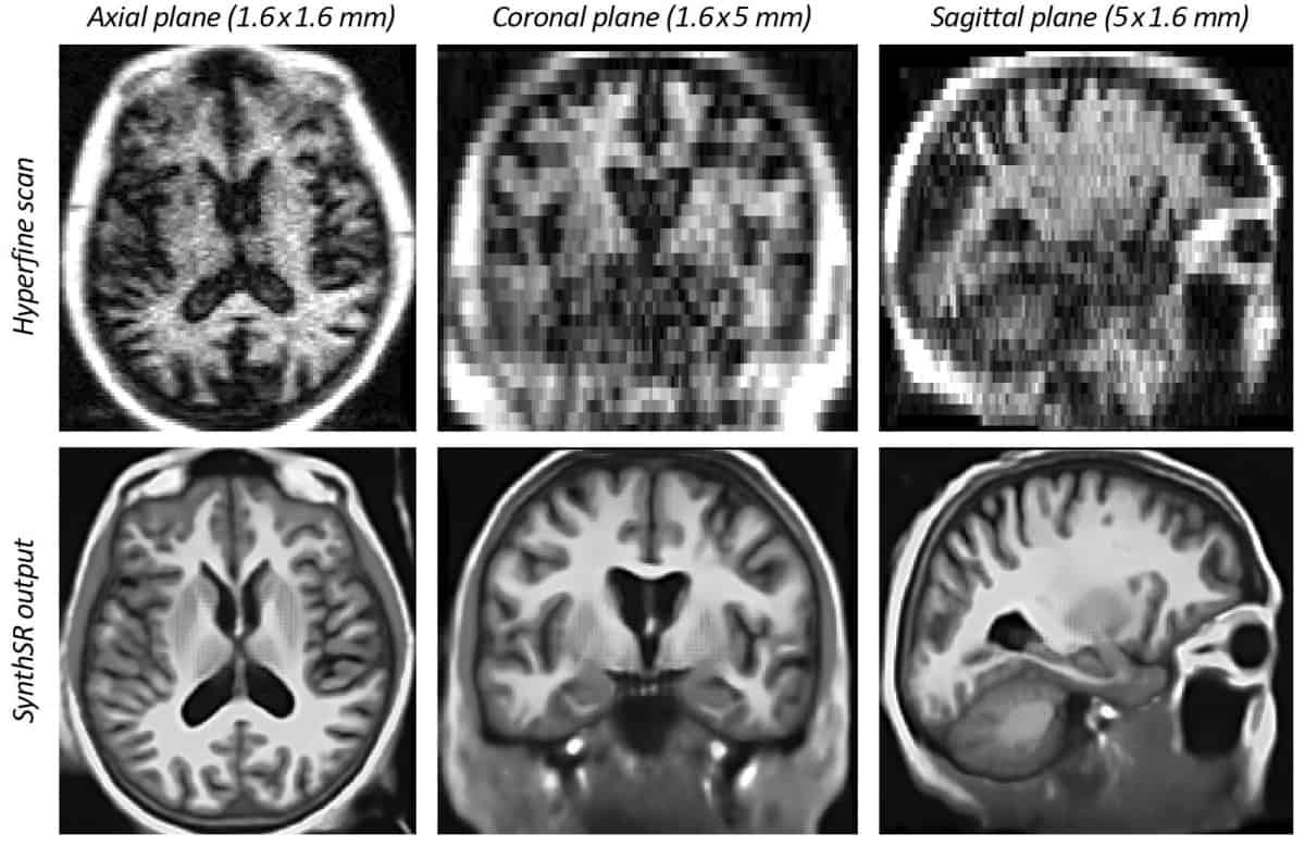
Image transformation Brain scan slices acquired with a portable, low-field Hyperfine MRI scanner (top row) and corresponding slices output by the LF-SynthSR algorithm (bottom row). The Hyperfine scan has 1.6 x 1.6 x 5 mm axial resolution, while the generated synthetic images have 1 mm isotropic resolution and are amenable to 3D analysis with automated morphometry tools. (Courtesy: Juan Eugenio Iglesias)
Portable, low-field-strength MRI systems have the potential to transform neuroimaging – provided that their low spatial resolution and low signal-to-noise (SNR) ratio can be overcome. Researchers at Harvard Medical School are harnessing artificial intelligence (AI) to achieve this goal. They have developed a machine learning super-resolution algorithm that generates synthetic images with high spatial resolution from lower resolution brain MRI scans.
The convolutional neural network (CNN) algorithm, known as LF-SynthSR, converts low-field-strength (0.064 T) T1- and T2-weighted brain MRI sequences into isotropic images with 1 mm spatial resolution and the appearance of a T1-weighted magnetization-prepared rapid gradient-echo (MP-RAGE) acquisition. Describing their proof-of-concept study in Radiology, the researchers report that the synthetic images exhibited high correlation with images acquired by 1.5 T and 3.0 T MRI scanners.
Principal investigator Juan Eugenio Iglesias from Massachusetts General Hospital and Harvard Medical School.
Morphometry, the quantitative size and shape analysis of structures in an image, is central to many neuroimaging studies. Unfortunately, most MRI analysis tools are designed for near-isotropic, high-resolution acquisitions and typically require T1-weighted images such as MP-RAGE. Their performance often drops rapidly as voxel size and anisotropy increase. As the vast majority of existing clinical MRI scans are highly anisotropic, they cannot be reliably analysed with existing tools.
“Millions of low-resolution brain MR images are produced every year, but currently cannot be analysed with neuroimaging software,” explains principal investigator Juan Eugenio Iglesias. “The main goal of my current research is to develop algorithms that make low-resolution brain MR images look like the high-resolution MRI scans that we use in research. I am particularly interested in two applications: enabling automated 3D analysis of the clinical scans and use with portable, low-field MRI scanners.”
Training and testing
LF-SynthSR is built upon SynthSR, a method developed by the team to train a CNN to predict 1 mm-resolution MP-RAGE isotropic scans from routine clinical MR scans. Previous findings reported in NeuroImageshowed that SynthSR-generated images could be reliably used for subcortical segmentation and volumetry, image registration and, if some quality requirements are met, even cortical thickness morphometry.
Both LF-SynthSR and SynthSR are trained on synthetic input images of highly varying appearance generated from 3D segmentations, and can thus be used to train CNNs for any combination of contrast, resolution and orientation.
Iglesias points out that neural networks perform best when data appear approximately constant, but every hospital uses scanners from different vendors that are configured differently, resulting in highly heterogeneous scans. “To tackle this problem, we are borrowing ideas from a field of machine learning called ‘domain randomization’, where you train neural networks with synthetic images that are simulated to constantly change appearance and resolution, in order to obtain trained networks that are agnostic to the appearance of the input images,” he explains.
To assess the performance of LF-SynthSR, the researchers correlated brain morphology measurements between synthetic MRIs and ground-truth high-field strength images. For training, they used a high-field-strength MRI dataset of 1-mm isotropic MP-RAGE scans from 20 subjects. They also used corresponding segmentations of 36 brain regions-of-interest (ROIs) and three extracerebral ROIs. The training set was also artificially augmented to better model pathologic tissue such as stroke or haemorrhage.
The test set comprised imaging data from 24 participants with neurological symptoms who had a low-field strength (0.064 T) scan in addition to a standard-of-care high-field strength (1.5–3 T) MRI. The algorithm successfully generated 1-mm isotropic synthetic MP-RAGE images from the low-field strength brain MRIs, with voxels more than 10 times smaller than in the original data. Automated segmentation of the synthetic images from a final sample of 11 participants yielded ROI volumes that were highly correlated with those derived from the high-field strength MR scans.
“LF-SynthSR may improve the image quality of low-field strength MRI scans to the point that they are usable not only by automated segmentation methods but potentially also with registration and classification algorithms,” the researchers write. “It could also be used to augment the detection of abnormal lesions.”
This ability to analyse low-resolution brain MRIs using automated morphometry would enable the study of rare diseases and populations that are under-represented in current neuroimaging research. In addition, improving the quality of images from portable MRI scanners would enhance their use in medically underserved areas, as well as in critical care, where moving patients to an MRI suite is often too risky.
Iglesias says that another challenge is the wide range of abnormalities found in clinical scans that need to be handled by the CNN. “Currently, SynthSR works well with healthy brains, cases with atrophy, and smaller abnormalities like small multiple sclerosis lesions or small strokes,” he tells Physics World. “We are currently working to improve the method so it can effectively deal with larger lesions, like larger strokes or tumours.”
Writing in an accompanying editorial in Radiology, Birgit Ertl-Wagner and Matthias Wagner from the Hospital for Sick Children in Toronto comment: “This exciting technical development study demonstrates the potential to go low on field strength and aim high for spatial and contrast resolution using artificial intelligence.”
If you’re a fan of space travel, chances are that you’ve already got coffee-table books featuring photographs from NASA’s Apollo missions. So you might be wondering whether you really need another one to add to your collection. In my opinion, the answer is yes – and the reason you do is evident as soon as you open Apollo Remastered by Andy Saunders.
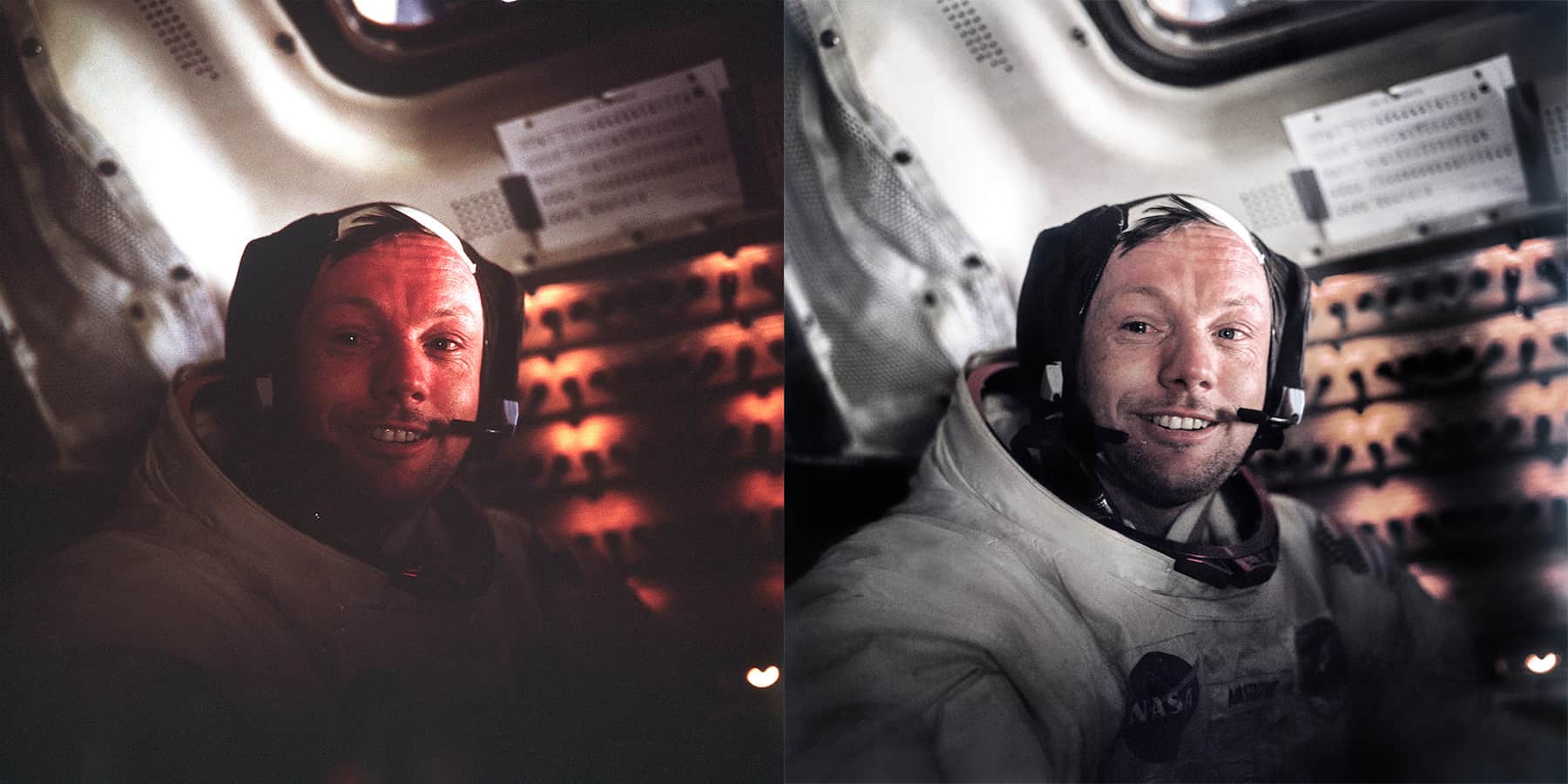
This glossy photograph book takes readers from NASA’s first human-spaceflight programme, Project Mercury, through to the final Apollo mission in 1972. By using modern photography restoration techniques, and having trawled through the 35,000 images that make up the NASA archive, Saunders brings new life to images we have long since cherished and, in some cases, have never seen before.
The reader is taken inside command modules with a clarity that reveals teary eyed crew members. We go on space walks with Gemini astronauts and are given astounding views of the Earth and the Moon. We see the space capsule that delivered Neil Armstrong and Buzz Aldrin to the Moon’s surface and are treated to a gate-fold pull-out of the Apollo 17 Moon buggy set in a panorama around Shorty Crater. Towards the back of the book, Saunders also includes chapters on the development of space photography and the equipment the astronauts used on those historic trips.
Before and after restoration A tired but elated Neil Armstrong in the Lunar Module after the historic first Moon walk. (Photo: Buzz Aldrin; courtesy: NASA; NASA /JSC /ASU /Andy Saunders)
While there is no shortage of books on the Apollo missions, Saunders has made this one stand out in a crowded field. In the chapter titled “About the scans, image processing and restoration”, he explains more about how he restored the film. It turns out that when the Apollo astronauts returned from the Moon, the film and photographs they took on their missions were duplicated and the original film placed in a secure vault in Building 8 at Johnson Space Centre (JSC).
The vault was maintained at 50% humidity and a temperature of 12.8 °C until 1982 when a new vault was built with a relative humidity of 20% and the film canisters were frozen at –18 °C. Freezing the film in this way slows down the rate at which the photos degrade, meaning they will survive for more than 500 years. Then, from 2008 onwards, staff at JSC and Arizona State University painstakingly took the frozen film out of the freezer, thawed it in a fridge at 13 °C and then digitized the images. It is from these scans that Saunders has produced the stunning images that fill the pages of this book.
I once spoke to Alan Bean, the Apollo 12 astronaut who later became an artist, painting the Moon and the adventures that he and his fellow astronauts had. Bean told me that, as an artist, you have to add a little colour that sometimes isn’t there. He would, for example, add colours to the surface of the Moon – just as Monet, say, would add colours to Rouen Cathedral, which is otherwise a plain, grey granite building.
“I can promise you,” Bean said, “we like those paintings a lot more than standing in front of a grey church.” Unlike Rouen Cathedral, however, the Moon is not actually uniformly grey – as the Apollo 17 astronauts discovered in 1972. While exploring the Shorty Crater, they found orange soil comprised of tiny glass beads that were created by volcanic activity. These patches of orange shine out from Saunders’ pages as delightfully as the colours in Bean’s paintings.
Panoramic view Harrison Schmidt unfolds the solar panels on the Surface Electrical Properties transmitter during Apollo 17. (Photo: Eugene Cernan; courtesy: NASA /JSC /ASU /Andy Saunders)
For Saunders, the goal of this book is to allow readers to see what the astronauts saw. In conversation with Apollo crew members, he has worked on aspects like colour balance and exposure to accurately represent the astonishing vistas. With no atmospheric haze, objects in the distance are as clear as those nearby. The balance of photographic manipulation is different for each image and the details are listed in the book’s captions.
But to deliver readers to the surface of the Moon, it has also been a case of taking things away. The source material is certainly high enough resolution. The RAW output from the digital scans of Apollo’s original 70 mm Hasselblad frames is a 1.3 GB, 16-bit TIFF file, 11,000 pixels square. Analogue stills for a digital world, though, mean that the raw images are underexposed, and adjusting them reveals relics and imperfections. Moon dust in the cameras are particular to these missions along with regular issues like the Sun affecting the film and photographs.
Each image is a feast for the eyes and, personally, I could spend a long time gazing into and exploring page after page. With over 400 full-page photographs, Apollo Remastered not only requires a sturdy coffee table, but is a treasure trove that will be relished by fans of one of humanity’s greatest achievements. Meticulously working on each image, Saunders has delivered the reader a time capsule worthy of anyone’s reinforced book shelves.
A laser-controlled water-based switch that operates twice as fast as existing semiconductor switches has been developed by a trio of physicists in Germany. Adrian Buchmann, Claudius Hoberg, Fabio Novelli at Ruhr University Bochum used an ultrashort laser pulse to create a temporary metal-like state in a jet of liquid water. This altered the transmission of terahertz pulses over timescales of just tens of femtoseconds.
With the latest semiconductor-based switches approaching fundamental upper limits on how fast they can operate, researchers are on the hunt for faster ways of switching signals. One unexpected place to look for inspiration is the curious behaviour of water under extreme conditions – like those deep within ice-giant planets or created by powerful lasers.
Molecular dynamics simulations suggest water enters a metallic state at pressures of 300 GPa and temperatures of 7000 K. While such conditions do not occur on Earth, it is possible that this state contributes to the magnetic fields of Uranus and Neptune. To study this effect closer to home, recent experiments have used powerful, ultrashort laser pulses to trigger photo-ionization in water-based solutions – creating fleeting, metal-like states.
Liquid jet
In the study, the trio in Bochum fired laser pulses at a water-based solution of sodium iodide. The solution was sprayed from a specialized nozzle, which flattened the liquid jet into a micron-thick sheet. When subjected to an intense optical laser pulse that lasted for 50 fs, electrons from the iodide ions become excited into the conduction band of the liquid water. This “pump” pulse makes the water behave like a metal, at least temporarily.
While in this metal-like state, the water’s optical properties are temporarily altered. To detect this change Buchmann, Hoberg and Novelli fired a “probe” pulse of terahertz radiation at the water and measured how much of the probe pulse was transmitted though the water. When the pump and probe pulses overlapped with zero delay, they found that the transmission fell by 20% compared to transmission in the absence of a pump pulse. By increasing the delay between the pump and probe, the team determined that it took just 70 fs for the water to relax from a metal to its normal state.
The terahertz probe pulses were about 1 ps long, which is significantly longer than the pump pulse and the relaxation time of the water. This allowed the team to change the shapes of the transmitted probe pulses, shifting the frequencies in the pulses to higher values. The trio says that this frequency-shifting effect could have useful applications in experiments.
Looking further into the future, the trio hopes that its research could pave the way for a new field of “water electronics”. With switching time of just 70 fs, water is already twice as fast as the best semiconductor switches, which take about 150 fs to change state.