Surgeons performing operations may orient themselves in the human body using sight and touch, but human senses can’t isolate things like small groups of cancer cells. Researchers at the University of Illinois at Urbana-Champaign tackled this challenge by developing a new image sensor that supplements a surgeon’s sight – and it’s based on how mantis shrimp see the world.
A multi-layered sensor the size of a postage stamp
Mantis shrimp have the most complex visual systems ever studied (they even hold a world record). Their compound eyes have three layers of photoreceptor cells, and each layer responds to a slightly different wavelength of light. All in all, mantis shrimp have up to 16 different types of photoreceptors.
Humans, by contrast, have only three colour vision photoreceptors (red, green, blue) that respond to visible light. To accommodate human vision, conventional image sensors often separate a single layer of photosensitive material into sections. Since each section is sensitive to a different wavelength of light, how much a surgeon sees using a camera – and the resolution of the images produced – is limited by how many sections an image sensor has.
The mantis shrimp, along with a magnified photo of its compound eye. (Courtesy: Sci. Transl. Med.)
Steven Blair, a graduate student in the lab of Viktor Gruev and lead author of a study published in Science Translational Medicine, has developed an image sensor the size of a postage stamp that, like the mantis shrimp’s eye, has not one but three layers of photosensitive material.
A camera using the sensor can display, with high resolution and when combined with two light-filtering materials, up to six colours of visible and near-infrared light. This could enable surgeons to use a single camera to isolate structures in the human body that might otherwise go unseen.
Filters and dyes
Surgeons who want to see the otherwise unseen can inject fluorescent dyes into a patient. The dyes bind to hidden tumour cells, for example, and emit visible or near-infrared light from structures that might have tumour cells in them. Conventional image sensors collect the light and create a real-time video feed that displays images from either the visible or near infrared that surgeons can refer to while operating.
But what if surgeons need to see the visible and near infrared light at the same time, as is the case when structures are located both near the surface and deep within the body? The researchers solved this problem by depositing two light-filtering materials on the top layer of their sensor, allowing them to capture colour and near-infrared images simultaneously.
“You may want to distinguish multiple tissues in the operating room,” says Blair. “Our sensor can visualize multiple fluorescent dyes and can thus provide a surgeon with a map of all of these tissues.”
Bio-inspired camera in the OR
To check how their sensor performed, the researchers built a camera by attaching a lens, electronics and housing to the sensor. They connected the camera to an external display so they could see the real-time video feed of overlaid colour and near-infrared images. The researchers demonstrated that their camera could visualize two hallmarks of cancer, abnormal cell growth and abnormal glucose uptake, when two fluorescent dyes that target these hallmarks were injected into mice with prostate tumours. They also could detect the tumours with greater accuracy using both hallmarks (dyes) together than each one alone.
Next, they brought their camera into the operating room. They found that the camera could pick up weak near-infrared light emissions under strong surgical lighting, which might help surgeons identify potentially cancerous lymph nodes near human breast tumours.
Because the camera is compact (approximately the size of a digital SLR), it can be integrated into an operating room. Pending regulatory approval of targeted dyes, the camera could be used to identify tumour boundaries as well as tumours, which could improve patient outcomes and shorten recovery times after surgery.
“Nature has developed an incredible diversity of different visual systems that are suited for all sorts of environments,” says Blair. “We looked at the inspiration that nature provided us and the tools that were available to us as engineers, and we developed a sensor that sort of found the middle ground between nature and engineering.”
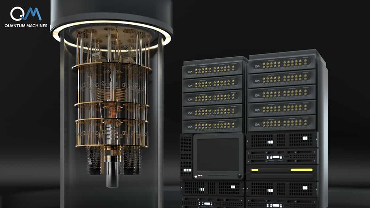
Quantum computing holds great promise for achieving immense computational power. While reaching the full potential of this paradigm presents considerable technical challenges, current Noisy Intermediate Scale Quantum (NISQ) devices have already demonstrated an advantage over classical hardware for particular computational tasks. Such demonstrations were achieved through incredible progress in designing quantum systems, engineering their environment, and controlling them effectively, leading to significant improvements in coherence times, gate fidelities, and the ability to integrate more qubits into a single quantum processor.
While the development of quantum hardware remains the primary challenge, many bottlenecks exist in the classical control hardware and software, where optimizations play a critical role for near-term quantum computing. This workshop introduces a new platform for implementing quantum control protocols, executing them on a wide range of quantum hardware, and optimizing their performance. This hardware and software solution, the Quantum Orchestration platform, combines a unique processor architecture that allows the most cutting-edge real-time control capabilities. We will demonstrate how the platform can control various setups and present live code use cases. Some examples will include feedback for error correction and repeat until success protocols; complex calibrations and optimizations; and hybrid quantum-classical algorithms.
Yonatan Cohen is a quantum physicist and entrepreneur, the CTO and co-founder of Quantum Machines. QM introduces Quantum Orchestration, a powerful platform to accelerate quantum research and development, and deliver unprecedented capabilities in quantum technologies. The platform empowers teams to realize the full potential of any quantum device. With its robust architecture and powerful yet intuitive programming language, QM makes it possible to run even the most advanced experiments and algorithms right out of the box. He is also the co-founder and the ex-managing director of the Weizmann Institute’s Entrepreneurship Program. Yonatan completed his MSc and PhD in Prof. Moty Heiblum’s lab at the Weizmann Institute of Science in Israel, working on quantum electronics, superconducting-semiconducting devices and microfabrication.
Gal Winer is a quantum physicist and the QUA libraries team lead at Quantum Machines. Gal did his PhD working on quantum optics in cold Rydberg atoms in the Weizmann Institute with Prof. Ofer Firstenberg. He has also worked in industry on metrology and automated optical inspection in semiconductor manufacturing.
A new device for rotating the polarization of terahertz radiation has been created by accident by researchers in the US. While practical applications remain unclear, the discovery could boost the bandwidth available to personal electronic devices like smartphones.
The terahertz region of the electromagnetic spectrum falls between the microwave and the infrared. It has numerous current and potential applications ranging from detecting concealed objects to telecommunications. However, the lack of convenient terahertz sources and other components has created a “terahertz gap” that has frustrated greater exploitation. Now, researchers at Rice University in the US may help close the gap by developing an ultrathin, broadband carbon-nanotube based device that can rotate the polarization of terahertz radiation by angles of 90° or more.
Controlling the polarization of electromagnetic radiation is crucial in numerous areas of science and technology. Control is particularly tricky in the terahertz region and rotating polarization usually involves a quartz wave plate about 1 mm thick.
“Even 1 mm is very thick to have as part of a modular device in something like a smartphone”, says Rice physicist Andrey Baydin, pointing out that this is an obstacle to using terahertz in consumer electronics like smartphones – which currently use microwave frequencies – in order to boost data transmission. Moreover, these waveplates have no tunability and work over an extremely narrow band of frequencies.
Aligned nanotubes
On reflection: diagram showing some of the terahertz pulse going straight through the sample and some of the pulse reflecting before emerging. (Courtesy: Kono Laboratory/Rice University)
In the new research, Baydin and colleagues chanced upon an alternative to the quartz wave plate after depositing a solution of aligned single-walled carbon-nanotubes (CNTs) onto a silicon substrate. The resulting nanotube film was analysed using terahertz time domain spectroscopy, in which a terahertz pulse is fired through a sample and the substrate behind. Some of the pulse goes straight through the sample and substrate and arrives at a detector. Some of the pulse is reflected at the silicon-air interface and goes back into the sample (see figure). There, it reflects from the CNTs and emerges again to be detected as a second pulse. This technique allows researchers to perform transmission and reflection spectroscopy simultaneously on their samples.
In their experiment the input pulse has a normal incidence on the sample, which the researchers rotated to vary the angle between the polarization of the input pulse relative to the orientation of the nanotubes in the film. They discovered that at a specific “magic” angle, the polarization of the second pulse was rotated exactly 90° relative to the input pulse. This magic angle was 30˚ in their sample, but its value depends on the thickness of the nanotube film and substrate, as well as the refractive index of the substrate.
Baydin says that their results came as a big surprise: “we were simply characterizing these nanotubes”.
Their curiosity piqued; the researchers created a mathematical model to gain a better understanding of the observed effect. “The refractive index and absorption coefficient are very different along the nanotubes and perpendicular to the nanotubes,” explains Baydin.
Broadband effect
As a result, the input pulse that approaches the nanotubes from one side behaves differently from the reflected pulse that approaches the nanotubes from the other side and at a different angle. This gives rise to the remarkable effects observed. The effect is more broadband than seen the traditional waveplates. Moreover, as the nanotube films are inherently anisotropic, dramatic variations in the properties of the surface should be achievable simply by rotating its angle relative to the light source.
“[Baydin and colleagues have] done a lot of work using carbon nanotubes as components in terahertz polarizers,” says Peter Armitage of Johns Hopkins University in the US. “Incorporating a thin-film geometry like this and silicon – which is a conventional material in the semiconductor industry – means one can take this kind of thing and incorporate it into terahertz-range optoelectronic devices. I wouldn’t say it’s an exotic effect but it’s quite remarkable that you can take these kinds of components, arrange them in this fashion, and get out this very large rotation of terahertz light.”
The next step, says Armitage, is “trying to incorporate these elements into actual devices”. Some of these devices, he says, may be laboratory ones. He gives the example of his own research, which involves using terahertz radiation to probe material properties. “The anisotropies in the polarization response tell us different things about a material,” he says. “For that, you don’t usually care if [your components] are bulky but you do usually care if they’re broadband. This is a way of treating all frequencies reasonably equally.”
A new material that is twice as magnetostrictive as others in its class could be a significant boon for computer-chip developers. The material’s unusual ability to expand and contract in response to tiny pulses of electric current has attracted interest from the chip manufacturer Intel, which is investigating possible replacements for the CMOS (complementary metal-oxide-semiconductor) technology that has dominated the industry for decades.
John Heron. Courtesy: University of Michigan
In today’s CMOS-based transistors, the semiconductor’s resistance changes when a voltage is applied across an insulating gate. This switching mechanism has long been the mainstay of electronics, remaining dominant even as transistors have shrunk down to mere nanometres in size. Reductions in the gate voltage and frequency, however, have not kept pace with reductions in chip size, and further decreases in operating voltages are unlikely because of the so-called Boltzmann limit of current control. Researchers are thus looking for alternative technologies.
Shape changes flip the magnetic field
One line of investigation concerns magnetostriction, or the tendency of an iron-containing material to expand and contract slightly as pulses of electric current are applied to it. Magnetostriction is associated with ferromagnetism and is perhaps best known as the source of the familiar hum that emanates from fluorescent lights and transformers. However, because changes in the shape of a magnetostrictive material also cause the material’s magnetic field to flip, this sometimes-irritating phenomenon could prove key to next-generation “magnetoelectric” devices.
Devices of this type would use such electrically-induced magnetic fields to store the digital one and zeros of binary data. Unlike conventional CMOS technology, these switching devices wouldn’t require a steady supply of electricity, so they should require much less energy to operate.
Unwanted order
Most magnetostrictive materials contain rare-earth elements, which are becoming too scarce and expensive to be used in the quantities required for chip manufacture. In the new work, researchers led by John Heron of the University of Michigan focused instead on an iron-gallium alloy with the chemical formula Fe1–xGax. Heron explains that the magnetostriction of this alloy normally increases with increasing concentrations of gallium. However, these increases eventually level off at around x = 19% before decreasing sharply as the higher amounts of gallium start to form an ordered intermetallic atomic structure.
To overcome this problem, the researchers used a process called low-temperature molecular-beam epitaxy to “freeze” the atoms in the compound, so preventing them from forming this unwanted order. This technique enabled the researchers to boost the fraction of gallium in the material to x = 30%, increasing its magnetostriction by tenfold compared to unmodified alloys.
“Spray painting”
Heron likens the technique, which is detailed in Nature Communications, to “spray painting” with individual atoms. The technique has a further advantage in that it allows the material’s magnetostrictive properties to be measured simply by applying it to a surface that deforms slightly when a voltage is applied.
The magnetoelectric devices in this study are several microns across, and the researchers acknowledge that this is large by today’s computing standards. However, they hope that their collaboration with Intel will help them shrink their devices down to a size that is compatible with the company’s magnetoelectric spin-orbit (MESO) device programme.
“Intel is great at scaling things and at the nuts and bolts of making a technology actually work at the super-small scale of a computer chip,” Heron says. “They’re very invested in this project and we’re meeting with them regularly to get feedback and ideas on how to ramp up this technology to make it useful in the computer chips that they call MESO.”
Heron and his colleagues have filed for patent protection on their technology through the University of Michigan’s Office of Technology Transfer.
We’ve all heard about the promise of quantum technologies to transform business and industry, whether it be for more secure communications networks or vastly more powerful computation. But what is needed to translate experimental quantum research into commercial success, and when can we expect it to happen?
According to speakers at the inaugural Quantum West conference, the transition from lab-based R&D towards market-ready solutions is already under way. While the headline-grabbing applications of quantum computing and the quantum Internet remain a longer-term bet, prototypes and products are already appearing in other areas of quantum technologies. One example is atomic clocks. Originally developed by the research community to provide more precise timing standards, the focus is now on re-engineering compact versions for use in high-speed mobile communications, synchronizing financial transactions, and other situations where accurate and resilient timekeeping offers a business advantage.
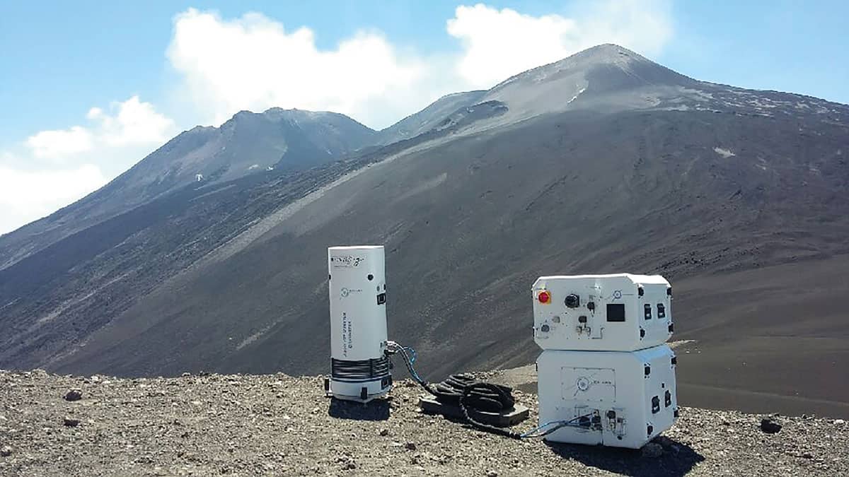
Applications for quantum sensors are also emerging. One notable example presented during the conference is a gravity sensor developed by Muquans, a French spin-off. Based on a Newtonian free-fall experiment in which a cloud of rubidium atoms cooled close to absolute zero is used as the test mass, Muquans’ system integrates all the key components into a single unit that is robust and reliable enough to be deployed in the field for geophysical monitoring – including on the slopes of Mount Etna.
“I sometimes hear the question about what will be the first real-life application of quantum technologies,” Muquans chief executive Bruno Desruelle told the Quantum West audience. “Well, there are already some quantum instruments that are in service now. We have built more than 10 units and we really believe that quantum technology offers a very interesting competitive advantage for gravity measurements.”
While the Muquans instrument is aimed mainly at the scientific community, other sensors are being developed for a mass market. As an example, the UK start-up QLM has demonstrated a gas sensor that exploits photon quantum statistics to detect methane emissions. Such a sensor could replace the manual sniffer tests currently used in oil and gas exploration to spot leaks of this greenhouse gas, and QLM chief executive Murray Reed says the company is set to produce handheld units costing less than £1000 within the next few months. The same technology could also be used to monitor emissions of carbon dioxide.
In the field French start-up company Muquans has built quantum gravity sensors based on a cold-atom experiment that is robust and reliable enough to be deployed on the slopes of Mount Etna. (Courtesy: Muquans)
Gateway to growth
The idea that early implementations of quantum systems for specific applications will pave the way for more ambitious commercial development is at the heart of the UK’s National Quantum Technology Programme (NQTP). In his keynote address, Peter Knight, who serves on the NQTP advisory board, described its approach: “We identified a kind of funnel of what we’re able to do in the very long term – for example, in quantum computing – and in the near term where we can pull out commercial and strategic value en route to achieving that long-term goal.”
The programme, which was among the first government-sponsored initiatives to recognize and encourage commercial opportunities for quantum technologies, identified four key areas where quantum technologies are likely to play an important role: sensing and timing, imaging, communications, and simulation and computing. For each area, it mapped out the commercial outcomes that could be achieved for each one over different timescales. In quantum communications, for example, a demonstrator project has already shown that quantum key distribution can be deployed in a standard fibre network, while ongoing NQTP-funded research focuses on developing quantum-resistant algorithms that will be needed to prevent attacks from next-generation quantum computers.
Matt Langione, a partner at the technology analytics firm Boston Consulting Group (BCG), delved deeper into the likely evolution of quantum computing, and its resulting market value, over the next 20 years. BCG’s analysts compared the business opportunities that more computational power would bring with the hardware and software innovations needed to deliver it – whether through improvements to classical computation or the introduction of quantum-powered solutions.
Within the next three to five years, BCG’s analysis suggests that early quantum processors with fewer than 1000 qubits, capable of tasks such as error mitigation and data compression, could deliver commercial value in four industry sectors: finance, pharmaceuticals, materials, and computational fluid dynamics simulations used in the automotive and aerospace industries. In this initial phase, Langione believes that the financial benefit for those four industries could reach a few billion dollars.
Further ahead, more sophisticated quantum computers – ones that exploit some level of error correction – will lead to a phase that Langione describes as offering a “broad quantum advantage”. Such fault-tolerant quantum computers are expected to emerge in a decade or so, and could be used in simulations that speed up materials design and reduce risk in financial trading. In the process, they might boost the overall commercial benefit to $25–50bn.
Beyond that, from about 2030, quantum computers with full-scale fault tolerance could solve the kind of problems that would completely transform the commercial outcomes from these four industries – for example by enabling the discovery of completely new drugs and materials, or allowing banks to make the most efficient use of their capital. At that point, Langione predicts that the market value generated by quantum computers would reach hundreds of billions of dollars.
Engineering a quantum future
Such views may seem optimistic, particularly when current research efforts focus on scaling up quantum processors from mere tens of qubits to the hundreds and thousands required to build fault-tolerant quantum computers. Indeed, a major emphasis of the talks at Quantum West was the urgent need to engineer practical and scalable systems for operating such complex quantum systems. Underlining the scale of the challenge was Google’s Eric Ostby, who revealed that at least 8000 additional components are currently needed to control and read out the 54 qubits in the company’s latest quantum chip.
More generally, engineering any practical quantum system will mean replacing today’s intricate experimental set-ups with robust and reliable plug-and-play units. Key to the success of the Muquans gravimeter, for example, is a bespoke laser technology that replaces optical components carefully arranged on an optical table with a solid-state frequency-doubling architecture that offers greater stability as well as easy integration with standard telecoms components.
This being Photonics West, many of the speakers focused on the crucial importance of photonics technologies for quantum applications. Lasers, for example, are widely used to manipulate quantum states, and over the last few years many devices have emerged with the narrow linewidths and wide tunability needed for quantum experiments. Even so, Scott Davis, chief executive of laser manufacturer Vescent Photonics, was candid about the shortfalls of the current generation of these devices. “There’s a gap between current laser reality and what the quantum system engineers want,” he said. “They are looking for something like a telecom package that’s cheap and fully integrated, while today’s devices only operate at certain wavelengths and are still really only designed for use in the lab.”
Part of the problem for companies such as Vescent is that there is no clear roadmap to guide their product development efforts. With this in mind, the Quantum Economic Development Consortium (QED-C), an organization that aims to support the growth of the US quantum industry, organized a workshop in September 2020 to discuss the future photonics requirements for quantum applications.
“One of the big takeaways is that the path forward for lasers for quantum is not so clear,” noted Davis, who chaired the workshop. “It’s a complicated space right now, with lots of different applications calling for different wavelengths and laser properties.” As a result, QED-C has launched an initiative to identify the technology and market intersections that should be tackled first.
Meanwhile, Davis is convinced that the best way to reduce the current market uncertainty is to get involved with academic research projects. Working in partnership with quantum scientists helps laser manufacturers to design devices that meet the specific technical requirements, from which they can engineer more integrated products that can be sold to equipment manufacturers. This has allowed Vescent to create, for example, an integrated laser-based system that has already been deployed in quantum sensors and atomic clocks.
Working together we can do so much more than working apart
Peter Knight
Many other speakers stressed the need for strong collaboration between industry, academia and government programmes to drive early commercialization efforts. This approach has already been formalized in some parts of the world, including the UK. Knight described the NQTP as building a “quantum alliance” between academic research groups (which focus on creating scientific knowledge), large and small companies (which can identify market opportunities and build practical solutions), and government (which functions as a sponsor and early adopter of quantum technologies). A measure of its success, Knight said, is that in a recent funding round for larger projects, 63 companies were involved in bids for the available £84m, and these businesses had themselves raised an additional £109m for quantum technology development over the last two years. “The appetite for working on this and translating the technology into the market is really there,” he said. “Working together we can do so much more than working apart.”
This June we will bring you Quantum Week – a series of free-to-attend scientific presentations in the field of quantum science and technology. Presentations will be on topics including quantum processors, the ethics of quantum computing and computational advantage. Find out more and register today.
Even if you’re not able to join the live events, registering now enables you to access the recordings as soon as they are available.
A bowling ball might look round on the outside, but inside there is a distinct departure from spherical symmetry. That is what I learned from reading a wonderful article on the physics of bowling balls – written by Brendan Koerner and published on the Wired website.
Called “One man’s amazing journey to the center of the bowling ball”, the article looks at the career of Mo Pinel, who revolutionized the design of bowling balls. In the early 1970’s he began experimenting with reducing the rotational symmetry of bowling balls. He first did this by drilling holes into the balls and filling them with materials with different densities. He realized that his modifications could improve how a ball was rolled but then drifted away from the idea to run a bowling-related business.
Fast forward many years later and Pinel decided to take a chance and commercialize his ideas. He created a ball with an asymmetric core that began to wobble back and forth (or flare) as it approached the end of the alley, knocking down more pins as a result. If you want to know the physics behind flaring, read Koerner’s article.
Hawking’s office
The cosmologist Stephen Hawking died in 2018 and now his archive, some personal belongings, and the contents of his office at the University of Cambridge have been acquired for the people of the UK in lieu of taxes owed by Hawking’s estate. The office contents will go to the Science Museum in London to settle a £1.4 million tax debt while the archive will go to Cambridge University Library to settle £2.8 million.
According to The Guardian, the office contents include Hawking’s personal reference books, blackboards, coffeemaker, medals and Star Trek mementoes. The Science Museum will also get six of Hawking’s wheelchairs and the technology he used to communicate after he was unable to speak. The archive includes television scripts from The Simpsons, in which Hawking appeared.
The Science Museum will display some of the items in 2022 and plans to recreate Hawking’s office
Recent advances in materials, mechanics, and manufacturing establish the foundations for high-performance classes of microfluidic lab-on-a-chip technologies that have physical properties matched to those of human skin. The resulting devices can integrate with the surface of the skin in a water-tight yet physically imperceptible fashion, to provide continuous, clinical-quality biochemical information on physiological status via capture, storage, and in situ analysis of sweat.
This webinar, presented by John Rogers, summarizes key ideas and presents specific recent examples in skin-interfaced microfluidic technologies designed for applications in sports performance, worker safety, and nutritional monitoring.
Prof. John A Rogers received his BA and BS in chemistry and physics from the University of Texas, Austin, in 1989. At the Massachusetts Institute of Technology, he completed an SM in physics and chemistry in 1992, and PhD in physical chemistry in 1995. From 1995 to 1997, Rogers was a junior fellow in the Harvard University Society of Fellows. He joined Bell Laboratories as a member of technical staff in the Condensed Matter Physics Research Department in 1997, and served as director of this department from the end of 2000 to 2002. He then spent 13 years on the faculty at the University of Illinois, most recently as the Swanlund Chair Professor and Director of the Seitz Materials Research Laboratory. In the fall of 2016, he joined Northwestern University as the Louis Simpson and Kimberly Querrey Professor of Materials Science and Engineering, Biomedical Engineering and Medicine, with affiliate appointments in mechanical engineering, electrical and computer engineering and chemistry, where he is also director of the recently endowed Querrey Simpson Institute for Bioelectronics. He has published more than 750 papers, is a co-inventor on more than 100 patents, and co-founded several successful technology companies. His research has been recognized by many awards, including a MacArthur Fellowship (2009), Lemelson-MIT Prize (2011), National Security Science and Engineering Faculty Fellowship (2012), Smithsonian Award for American Ingenuity in the Physical Sciences (2013), MRS Medal (2018), and the Benjamin Franklin Medal from the Franklin Institute (2019). He is a member of the National Academy of Engineering, National Academy of Sciences, National Academy of Medicine, National Academy of Inventors, and the American Academy of Arts and Sciences.
Scientists in the US have produced a detonation that is fixed in space for the first time. This standing wave detonation was created in a prototype engine and the researchers say that such a system could one day power aircraft at up to 17 times the speed of sound.
Most fires are deflagrations. This form of combustion creates a subsonic reaction wave and powers much of our transport technology. But you can get a much more powerful and efficient release of energy from a detonation. This type of combustion produces supersonic shock waves driven by energy release from closely coupled chemical reactions. These waves travel at many times the speed of sound, with those produced by igniting a hydrogen–air fuel mix, for example, often reaching speeds of Mach 5.
This intense energy release is highly unstable and difficult to control. If harnessed, however, it could be channelled to achieve hypersonic flight for future interplanetary travel and ultrahigh-speed intercontinental travel on Earth. Estimates suggest that an engine operating with a Mach 5 flow path, such as that produced by a hydrogen–air fuel mix, could enable vehicle speeds of Mach 6 to 17. That would allow you to fly from New York to London in just half-an-hour.
There are three main detonation engine concepts. Pulse detonation engines create repeated explosions, while in a rotating detonation engine, detonations continuously travel around a circular channel with the shockwave from each setting off the next. Both of these have been previously demonstrated. Now, researchers at the University of Central Florida and the US Naval Research Laboratory say they have demonstrated the third concept: a standing or oblique detonation wave engine. They report their results in the Proceedings of the National Academy of Sciences.
The idea behind an oblique detonation wave engine is to produce a continuous detonation that is fixed in space, so that the resulting shockwave is stable and remains in the same position. “We want to feed [the detonation] with the right propellant mixture, at the right speed and freeze it in space,” Kareem Ahmed tells Physics World.
To create such a detonation, Ahmed and his colleagues developed a prototype engine named HyperReact (high-enthalpy hypersonic reacting facility). This device is divided into three sections. In the first, the mixing chamber, a jet of hydrogen and air is ignited. This creates hot high-pressured air that flows into the next section, the converging–diverging (CD) nozzle, which has an axisymmetric square cross-section along its entire length. As the air enters the CD nozzle a jet of ultrahigh-purity hydrogen is added. The shape of the CD nozzle is designed to then accelerate the mixture to speeds of around Mach 4.5 as it enters the test section. In this final chamber there is a 30-degree turning angle ramp.
The team found that by manipulating the fuel mix, temperature and air flow through the chambers they were able to produce an oblique shock on the ramp that created a detonation that was stabilized on the ramp. This standing wave detonation lasted for the duration of active fuelling, which was around three seconds. This is significantly longer than a normal detonation and demonstrates proof-of-concept, the researchers say.
Ahmed explains that the main benefit of detonation based propulsion would be much higher efficiency than deflagration-based systems. “Achieving hypersonic speeds is critical because we don’t currently have a propulsion system that can do that,” he adds. “The only propulsion system that can give you hypersonic speeds is a rocket motor. Now rocket motors are not efficient. We know that because otherwise we’d all be flying to outer space. They are very expensive.”
Ahmed tells Physics World that now the researchers have proved that an oblique detonation wave engine is possible they want to explore the different conditions, such as fuel type and speed of the fuel flow, under which the detonation can remain stable. This is necessary to achieve the levels of control that would be required to realise hypersonic flight.
Artificial intelligence (AI) technologies are designed to replicate human capabilities, and in some cases improve upon them. Lifelike robots are physical examples of AI technology, but it is the digital AI systems that already have a ubiquitous influence on our daily lives – from facial recognition software to decision-making tools used by banks, recruiters and the police. Too often, these systems can reflect preexisting social inequalities.
In this episode of the Physics World Stories podcast Andrew Glester investigates the ethical issues that can plague AI and machine learning technologies. He finds out about the concepts of deep learning and neural networks, why these systems can amplify problems in society, and who are the people adversely affected by these flaws.
It turns out that the physics community is part of the problem and potentially part of the solution. Directly and indirectly, physicists are involved in developing AI technology so are ideally placed to raise awareness of the issues. Featuring in the episode:
Alan Winfield, a robot ethics researcher at the University of the West of England
Julianna Photopoulos, a science writer based in Bristol, UK
Savannah Thais, an experimental particle physicist at Princeton University, US
To find out more about the issue of bias in AI systems, take a look at this feature article by Photopoulos, which is summarised in the video below.
Physicists at the Massachusetts Institute of Technology (MIT) in the US have found a new way to switch antiferromagnetism on and off. Their technique, which involves doping antiferromagnetic materials with extra electrons, could allow for faster, higher-density and more stable memory storage.
Riccardo Comin, who led the research. Courtesy: Comin Photon Scattering Lab
Modern hard disk drives encode data by using magnetic field pulses to flip the spins of electrons (representing binary zeros and ones) in ferromagnetic materials within computer chips. While researchers have found ways to switch these binary bits at ever-smaller scales, the magnetic pulses require a relatively large electrical current, so the data-writing process dissipates a lot of energy. It is also relatively slow, with a complete spin flip taking tens of nanoseconds.
Promising candidates
Antiferromagnetic materials are promising candidates for future high-density memory applications because the spins in antiferromagnets flip much faster, at frequencies in the terahertz range. These rapid spin flips are possible because of strong interactions between electron spins, which come about because the spins in antiferromagnets tend toalign so that they are antiparallel to each other (unlike conventional ferromagnets, which have parallel electron spins).
Antiferromagnets also lack magnetization on the scale of a single bit (>10 nm), making them robust to external magnetic perturbations. This means that data encoded in a memory device based on antiferromagnetic bits could not be erased magnetically. A further advantage is that antiferromagnets could be made into smaller transistors (and thus be packed more densely onto chips) than is possible with conventional transistor materials like silicon.
Creating oxygen vacancies
In the new work, MIT researchers led by Riccardo Comin set out to determine whether they could manipulate the antiferromagnetic properties of 100-nm-thick films of samarium and neodymium nickel oxide (SmNiO3 and NdNiO3) by doping them with extra electrons. While doping usually involves introducing impurities in a material to alter its electronic properties, in this case Comin and colleagues achieved what’s known as carrier doping by stripping the SmNiO3 and NdNiO3 of oxygen atoms. This process leaves two electrons behind for every oxygen removed, and the left-behind electrons redistribute themselves among the remaining oxygen atoms and the nickel.
During these experiments, the researchers monitored the films using advanced magnetic X-ray crystallography techniques to determine whether the material’s magnetic structure remained intact – in other words, whether the atomic spins retained their orderly anti-alignment and therefore their antiferromagnetism. Any reduction in the previously ordered magnetic structure, they explain, would be evidence that the doping was enough to switch off the material’s antiferromagnetism.
Sharp magnetic transition
The researchers say the antiferromagnetic order in rare earth nickelates like the ones they studied is remarkably robust to carrier doping – up to a point. Then, at a critical doping threshold of 0.21 electrons per nickel atom, the order suddenly collapses. This magnetic transition is sharp, similar to switching a transistor’s state from zero to one, and can be reversed by adding oxygen back into the material.
Comin says that, like conventional ferromagnetic bits, antiferromagnetic bits might be switched using voltage gates (a process in which a small voltage is applied to a bit to alter its electrical conductivity). He tells Physics World that this would allow rare earth nickelate materials to be employed in field-effect devices that could directly read/write operations on antiferromagnetic bits.
The researchers, who report their work in Physical Review Letters, say they now hope to gain better control over the magnetic switching process, optimize it for device applications and explore more exotic physical properties in the rare earth nickelate family for functional applications. They also plan to study other materials with potentially higher magnetic transition temperatures as potential platforms for a new magnetic storage technology.


 Yonatan Cohen is a quantum physicist and entrepreneur, the CTO and co-founder of Quantum Machines. QM introduces Quantum Orchestration, a powerful platform to accelerate quantum research and development, and deliver unprecedented capabilities in quantum technologies. The platform empowers teams to realize the full potential of any quantum device. With its robust architecture and powerful yet intuitive programming language, QM makes it possible to run even the most advanced experiments and algorithms right out of the box. He is also the co-founder and the ex-managing director of the Weizmann Institute’s Entrepreneurship Program. Yonatan completed his MSc and PhD in Prof. Moty Heiblum’s lab at the Weizmann Institute of Science in Israel, working on quantum electronics, superconducting-semiconducting devices and microfabrication.
 Gal Winer is a quantum physicist and the QUA libraries team lead at Quantum Machines. Gal did his PhD working on quantum optics in cold Rydberg atoms in the Weizmann Institute with Prof. Ofer Firstenberg. He has also worked in industry on metrology and automated optical inspection in semiconductor manufacturing.
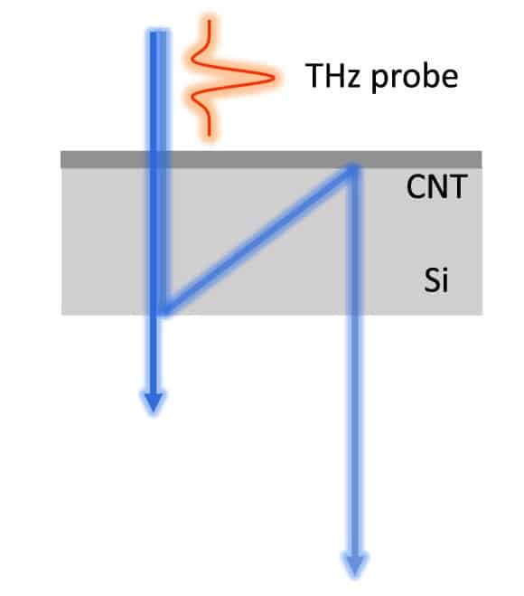

 Recent advances in materials, mechanics, and manufacturing establish the foundations for high-performance classes of microfluidic lab-on-a-chip technologies that have physical properties matched to those of human skin. The resulting devices can integrate with the surface of the skin in a water-tight yet physically imperceptible fashion, to provide continuous, clinical-quality biochemical information on physiological status via capture, storage, and in situ analysis of sweat.
 Prof. John A Rogers received his BA and BS in chemistry and physics from the University of Texas, Austin, in 1989. At the Massachusetts Institute of Technology, he completed an SM in physics and chemistry in 1992, and PhD in physical chemistry in 1995. From 1995 to 1997, Rogers was a junior fellow in the Harvard University Society of Fellows. He joined Bell Laboratories as a member of technical staff in the Condensed Matter Physics Research Department in 1997, and served as director of this department from the end of 2000 to 2002. He then spent 13 years on the faculty at the University of Illinois, most recently as the Swanlund Chair Professor and Director of the Seitz Materials Research Laboratory. In the fall of 2016, he joined Northwestern University as the Louis Simpson and Kimberly Querrey Professor of Materials Science and Engineering, Biomedical Engineering and Medicine, with affiliate appointments in mechanical engineering, electrical and computer engineering and chemistry, where he is also director of the recently endowed Querrey Simpson Institute for Bioelectronics. He has published more than 750 papers, is a co-inventor on more than 100 patents, and co-founded several successful technology companies. His research has been recognized by many awards, including a MacArthur Fellowship (2009), Lemelson-MIT Prize (2011), National Security Science and Engineering Faculty Fellowship (2012), Smithsonian Award for American Ingenuity in the Physical Sciences (2013), MRS Medal (2018), and the Benjamin Franklin Medal from the Franklin Institute (2019). He is a member of the National Academy of Engineering, National Academy of Sciences, National Academy of Medicine, National Academy of Inventors, and the American Academy of Arts and Sciences.