

China’s Beijing Graphene Institute looks to accelerate the ‘graphene era’

Zhongfan Liu

What is the role of the Beijing Graphene Institute (BGI) and why was it created?

Officially opened in 2018, the BGI is committed to building a world-leading graphene R&D cluster and developing the worldwide graphene industry. Graphene is an emerging strategic material and while the roadmap to industrialization is long and full of challenges, the BGI is aiming to accelerate it through a collaboration between government, industry and academia. We believe we are on the eve of a “graphene era”.

Who funds the institute?

The BGI is jointly funded by the Beijing municipal government and social capital funds with 320m RMB ($50m) as registered capital and about 200m RMB invested each year. The institute comprises two legal entities – a research centre that receives funding from local governments and a company focusing on business development.

We believe the best is yet to come. Graphene has a big potential in many applications

How many people work at the institute and is that set to grow in the future?

We currently have around 250 staff, which is growing at a rate of about 100 new staff every year. Despite its short history, BGI has been successful in attracting people and we aim to reach a thousand staff in the coming decade.

Why graphene?

Carbon-based materials have proved promising and have derived various industrial applications such as carbon fibre, graphite and activated carbon. Graphene, being another revolutionary carbon material, has shown promise due to its unique characteristics in terms of strength, electronic and thermal whilst being lightweight and transparent. The future for the industrialization of graphene is bright because of its extraordinary structural, physical and chemical properties.

What attracted you to graphene?

I started research in graphene in 2008. Before then I worked at Peking University on carbon nanotubes research. However, after publishing almost 600 research papers, I started to realize the limitation of fundamental research and think about doing something beyond that. Then in 2010 Andre Geim and Konstantin Novoselov shared the Nobel Prize for Physics for discovering graphene.

And how did that transform work on graphene?

Researchers around the world then began clamouring for ways to use this remarkable “supermaterial”. China also fell into “graphene fever” and began to create various graphene industrial parks and companies. Initially, the overfocus was irrational and concerning, so in 2016 I decided to set up the BGI to bring graphene research on the right path and pave the way for further industrialization. I hope BGI can follow the example of the Japanese company Toray, which leads the exploration of carbon fibre material and nurtures a worldwide carbon fibre industry.

What applications of graphene are you working on at the institute?

We are currently focusing on materials such as A3 sized super-clean graphene film, 4-inch single-crystal graphene wafers, graphene-coated glass fibres as well as 30 × 30 cm2 super graphene glass. These types of materials can be used in light-emitting diode devices, fibre-optic sensors, ultrafast lasers, high-performance heaters and more other areas. We aim to develop green and mass production techniques to make low-cost graphene materials, and to explore applications of graphene in traditional and high-tech industries.

How will these be scaled-up for applications?

We hope to build mass-production lines for the best quality materials, including manufacturing and characterization equipment as well as strong commercialization team, which can move these materials from the lab to the marketplace.

What do you think are the most exciting potential applications of graphene?

We believe the best is yet to come. Graphene has a big potential in many applications. But like carbon fibre, which was initially used in fishing pole and golf clubs before it found use in civil aviation, it takes time to explore the ultimate application of graphene. It will need joint efforts from researchers and entrepreneurs who are devoting themselves to the commercialization of materials.

What challenges – both technological and commercial – does graphene have to overcome to make it in these applications?

According to a report in 2018, most of the companies worldwide claiming to produce “graphene”, are producing less than 10% of the graphene (Adv. Mater. 30 1803784). This lack of properly characterized, high-quality material has been stalling the development of applications that depend fundamentally on graphene such as advanced coatings and composites, high-performance batteries, sensors as well as electronic and optoelectronic devices. Another challenge we are facing is to find an ultimate application for graphene and then nurturing that market.

Do you work with international collaborators or companies?

The BGI has been working with many academic institutes in Europe by providing graphene and single crystal graphene wafers for LED lighting devices. No commercial collaborations have begun yet.

What would mark success for the institute over the next 5-10 years?

The BGI is aiming to be leading player in a graphene industry that is set to be worth over $100bn. We also want to be an integrated enterprise that incubates multiple subsidiaries in different areas.
Transistor-like device controls graphene’s electronic properties

Researchers in Germany and Spain have created a transistor-like device that uses a small voltage to control the strength and frequency of electronic signals transmitted through graphene. The feat, which is detailed in Science Advances, marks an important step towards using graphene in electronic devices such as terahertz frequency converters, mixers and modulators.

Graphene – a honeycomb-like lattice of carbon just one atom thick – has several unique electronic properties. Many of them stem from the fact that it is a semimetal with no energy gap between its valence and conduction bands. In the region where these two bands meet, the relationship between the energy and momentum of charge carriers (electrons and holes) in graphene is described by the Dirac equation, rather than the standard Schrödinger equation as is the case for most crystalline materials.

High electronic conductivity and massless behaviour

The presence of these unusual band structures (known as Dirac cones) enables the charge carriers in graphene to behave like massless particles. This effective masslessness gives the electrons in graphene a very high mobility – up to 200 000 cm2/Vs at room temperature, compared to only about 1400 cm2/Vs in silicon. Such extremely high mobility means that graphene-based transistors and other electronic devices could be faster and more energy efficient than any that exist today.

Researchers recently discovered that when an electric current (or a light wave) passes through graphene, the material’s high electron conductivity and the effectively massless behaviour of its electrons changes the frequency of the current. This type of nonlinear behaviour is one of the most basic functionalities in modern electronic devices, crucial for switching and processing electrical signals.

Graphene’s nonlinearity is by far the strongest of all electronic materials, notes Dmitry Turchinovich of Bielefeld University, who co-led the latest study with Michael Gensch of the German Aerospace Center (DLR) Institute of Optical Sensor Systems and the Technical University of Berlin. The material also remains highly nonlinear even at high frequencies, extending into the technologically important terahertz (THz) range where most conventional electronic materials fail.

Tight control

While this behaviour is important for integrating graphene into electronic devices, researchers need to be able to control it first. Gensch, Turchinovich and colleagues have now demonstrated that such control is possible. In the new work, they fabricated a transistor-like device to which they could apply a gate (control) voltage via electrical contacts. They then used the device to transmit ultrahigh frequency THz signals and analysed how the frequency of these signals transformed as a function of the applied voltage.

At a certain applied voltage, the researchers observed that graphene’s normally strong nonlinear response nearly vanished. By slightly increasing or decreasing the control voltage from this critical value by just a few volts, they found they could make the material strongly nonlinear again. Once they determined the optimal gating voltage, they showed that they could alter the strength and the frequency components of the transmitted and reemitted THz electronic signals by as much as two orders of magnitude.

A missing link

Being able to control graphene’s nonlinearity in such a simple way is the “missing link” for using the material in electrical signal processing and signal modulation applications, Turchinovich says. “With this work, we have reached an important milestone on the path towards using graphene as an extremely efficient nonlinear functional quantum material in devices like THz frequency converters, mixers, and modulators,” Gensch adds.

Gensch goes on to explain that graphene is also perfectly compatible with existing electronic ultrahigh-frequency semiconductor technology such as CMOS or Bi-CMOS. It is therefore possible to envision hybrid devices in which the initial electric signal is generated at lower frequency using existing semiconductor technology, and is then very efficiently up-converted to much higher THz frequencies using graphene – all in a fully controllable and predictable manner.

The team, which also includes researchers from the Helmholtz Center Dresden-Rossendorf, the Max Planck Institute for Polymer Research and the University of Duisburg-Essen in Germany and the Catalan Institute of Nanoscience and Nanotechnology (ICN2) and the Institute of Photonic Sciences (ICFO) in Spain, says it is now working on integrating graphene into SiGe HBT/Bi-CMOS chip technology.

Laser paints a mini masterpiece, counting bubbles in a glass of beer, Jane Austen written in oligomers

Vividly coloured paintings have been created by researchers in Russia by using a laser to heat the surface of a metal until it begins to evaporate. Developed by Vadim Veiko, Yaroslava Andreeva and colleagues at ITMO University in Saint Petersburg, the technique makes colours by creating oxide layers on the metal surface. The palette of nine basic colours can be created, erased and changed using the laser and the team used the technique to make a 7×5 cm reproduction of Vincent van Gogh’s The Starry Night in just a few minutes.

The team now hope to incorporate the laser-painting technology into a handheld tool and describe their research in Optica.

Have you ever wondered how many bubbles there are in a glass of beer? Gérard Liger-Belair and  Clara Cilindre did, and now they have an answer. The duo, which had previously counted bubbles in a champagne flute, first measured the carbon dioxide content of a freshly-poured glass of lager at 5 °C. Then they calculated how many bubbles would form at defects in the glass that are more than 1.4 micron wide. High-speed photographs revealed how bubbles grew as they rose in the glass, removing more carbon dioxide from the beer.

Glass imperfections

Putting all of this together, they reckon that between about 200,000 and nearly two million bubbles are created in a gently poured glass of lager before it goes flat. Interestingly, they discovered that beer and champagne bubbles form differently in a glass, with larger imperfections leading to more bubbles in beer but not in champagne. The researchers, based at the University of Reims Champagne-Ardenne, describe their study in ACS Omega.

Austenites have a new way of reading their favourite author now that a passage from Jane Austen’s novel Mansfield Park has been encoded in a series of oligomer molecules. Eric Anslyn and colleagues at the University of Texas at Austin used a new molecular-data-storage technique to encode the quote, “If one scheme of happiness fails, human nature turns to another; if the first calculation is wrong, we make a second better: we find comfort somewhere”.

According to the team, the words of wisdom can be read back without prior knowledge of the structures that encoded the passage. You can read more about the encoding technique in Cell Reports Physical Science.


New device can detect airborne virus particles that cause COVID-19, says maker

A device claimed to detect the virus that causes COVID-19 in ambient air within 2–3 min has been successfully tested at two universities in the US. It was developed by the company Smiths Detection, which says that the test has a sensitivity equivalent to PCR testing. The test is now commercially available in the US and is being prepared for a global rollout.

The ideal way of testing for the SARS-CoV-2 virus is using the reverse transcriptase polymerase chain reaction (RT-PCR or often just PCR). This involves taking a sample from the patient, using one enzyme to transform the viral RNA into DNA before thermally separating that DNA into single strands. The complementary fragment is then added to a sequence of the helix found only in the virus, recreating a short section of double helix if and only if the virus is present. Finally, this is amplified to produce a positive result.

Although a well-established technique, PCR can take days to produce a result – days during which an infected patient may infect others. Tests that can analyse samples more rapidly tend to be less sensitive. Moreover, an asymptomatic patient may have no reason to provide a sample for testing. A product that could rapidly detect SARS-CoV-2 in the ambient air would therefore be highly valuable, and several academic research groups and companies are working towards that aim.

Smiths Detection developed their BioFlash Biological Identifier over 10 years ago to detect toxins such as ricin and pathogens like the anthrax bacterium. The device is currently used by the US government and commercial companies such as couriers.

Jellyfish genes

“Previously, our focus was on biothreats that were intentionally released,” explains Andrew Flannery, one of the company’s chief scientists. The system uses a technology called CANARY developed by researchers at Massachusetts Institute of Technology. Genetically engineered immune cells bind to one specific target such as a toxin or pathogen. When they do so, they begin to emit light: “When CANARY technology was originally developed, [the MIT researchers] basically cloned out the same genes that jellyfish use to be bioluminescent,” explains Flannery. In addition to BioFlash, Smiths Detection has used the CANARY platform in sensors to detect pathogens in food and to monitor the health of plants in agriculture.

The company realized that, if the BioFlash could detect SARS-CoV-2, it could defend not just against malicious threats but against unintentional ones posed by infected individuals too. “We had to identify antibodies that would bind specifically to SARS-CoV-2,” explains Flannery, “We had to screen several antibodies that would be resistant to any mutations that might happen and lead to false negatives to make sure we picked the right one. That way we can be sure that, even if there are variants that pop up, we will still be able to detect them.”

The company now reports two real-world tests: one at the University of Maryland, Baltimore and the other at the University of Oregon. The first Maryland result detected the presence of SARS-Cov-2 in a locker room, leading to three positive diagnoses among members of a sports team, whereas the second confirmed its absence in a research facility in which a member had tested positive for COVID-19. The Oregon experiment detected the virus exhaled by quarantined patients with confirmed COVID-19.

Confirming virus mitigation

“Ultimately, we want to be part of the overall covid mitigation strategy,” says Warren Mino, the managing director of biotechnology at Smiths; “Having a device that will confirm that their mitigation strategies are working, I think, helps people to know that what they’re doing is effective in keeping people safe – especially as we try to get back to our daily, regular lives.”

Laura Lechuga of the Catalan Institute of Nanoscience and Nanotechnology, whose group has developed a spectroscopic liquid biosensor for SARS-Cov-2, is cautiously impressed: “As far as I know, there is no solution for on-site detection of SARS-CoV-2 in air (or aerosols) commercially available. There are many developments on-going at academic research and industrial level, but no one is close to commercialization. So, this Smiths device could become the first detector and could be [in massive demand],” she says. She cautions, however, that “the detection of any pathogen in air is really complex, due to the influence of the way the air sampling is performed, the specificity (to avoid cross-reactivity with other biomolecules and chemical molecules in the air) and, more importantly, the sensitivity level, as normally pathogens are present in the aerosols at a very low level”.

Lechuga adds that there is not currently enough public information available for her to evaluate the device. Smiths Detection told Physics World that the relevant proprietary information is provided to prospective customers.

ExoSCOPE monitors cancer treatment in real-time at the molecular level

The ExoSCOPE platform

Catching cancer drugs in the act may seem complicated – but could soon become a lot simpler.

One of the three common methods of treating cancer is chemotherapy; this process uses active chemicals to destroy abnormal or tumour cells. The fundamental challenge with chemotherapy is that it interacts with all rapidly dividing cells in the body, and therefore can cause severe side effects.

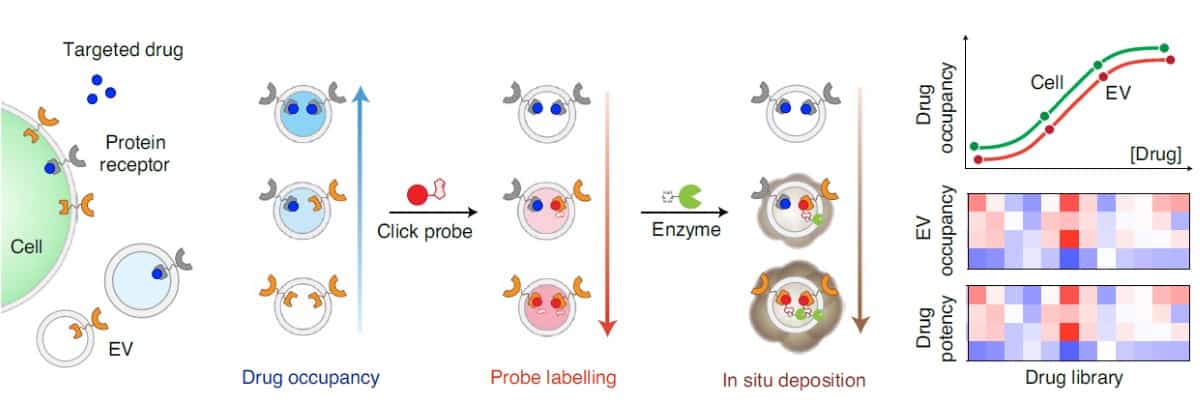
To improve on the downside of chemotherapy and other targeted therapies, scientists at the Institute for Health Innovation & Technology, National University of Singapore, have developed a treatment monitoring technology that evaluates specific drug interactions with cancer cells. The researchers describe the technology, named extracellular vesicle monitoring of small-molecule occupancy and protein expression (ExoSCOPE), in Nature Nanotechnology.

The ExoSCOPE technology

ExoSCOPE relies on the tiny nanoparticle-like vesicles secreted by mammalian cells, particularly cancerous cells. These so-called extracellular vesicles (EVs) contain several components, including the ones responsible for drug interaction and targeting. The ExoSCOPE technology examines the abundance of EVs produced in the blood, using plasmonic sensors to evaluate how drugs or other agents bind with EVs through specific protein receptors. This helps the researchers understand and monitor how cancer cells interact with drugs at the molecular level.

The team designed specialized probes consisting of gold nanorings, which were used to identify the docking sites of the drugs with the cancer cells.  Compared with a previously designed probe, these nanorings, which act as plasmonic resonators, offer enhanced signal detection by amplifying capture sites of molecular reactions with cancerous cells.

The new probe can amplify signals from EVs with low capacity for drug targeting and enables real-time monitoring of molecular reactions during ongoing cancer treatment. Plasmonic resonators generate electromagnetic hotspots, which maximize detection sensitivity. To increase signal detection, the team ensured that the molecular reactions occurred within these hotspots.

Clinical applications  

The team analysed plasma samples from lung cancer patients using the plasmonic nanoring resonators to identify possible cancer markers. Compared with other EV analyses, the ExoSCOPE results showed the most accurate disease classification, with an area under curve of 0.982.

The researchers further examined blood samples from lung cancer patients undergoing targeted treatment with erlotinib, to determine time changes in drug occupancy in cancer associated EVs. They note that the ExoSCOPE platform was able to differentiate between treatment outcomes (responders and non-responders) after just a 24 hrs time-lapse, whereas conventional blood pharmacological analysis could not.

“This technology offers a promising approach for monitoring treatment outcomes in cancer cells,” says first author Sijun Pan.

One step closer to real-time MR imaging in proton therapy

Proton therapy is an advanced cancer treatment technique that delivers highly targeted dose to the tumour while sparing surrounding normal tissue, enabled by the finite range of the proton beam. This precision targeting, however, is compromised by tumour motion or anatomical changes throughout a course of treatment. The absence of fast imaging tools to localize moving targets during dose delivery is a fundamental barrier to exploiting the full potential of proton therapy.

Real-time imaging during treatment delivery could visualize the tumour and synchronize the proton beam to its motion. MRI, which has recently been integrated into conventional photon-based radiotherapy systems, could provide high-resolution, high-contrast soft-tissue imaging, without depositing any additional ionizing dose into the patient. But operating an MRI scanner in conjunction with a proton beam is a major technological challenge that, for a long time, many considered to be impossible.

Aswin Hoffmann from the HZDR Institute of Radiooncology – OncoRay in Dresden thought otherwise. Hoffmann and his colleagues have been working for several years to integrate MRI with proton therapy. Now, the team is planning to build the world’s first whole-body prototype proton therapy system that can track moving tumours with MRI, in real time, during dose delivery from an actively scanned proton pencil beam.

The major challenge when integrating MRI into a proton therapy system is that MRI scanners need precisely defined magnetic fields to create geometrically accurate images, while proton therapy systems use electromagnetic fields to generate, transport and deliver the proton beam. Interference between these fields could distort the MR image and impact the delivered proton dose distribution. Hoffmann and his team showed that it is technically possible to combine both systems, and that these interference effects can be anticipated and thus compensated for. They also recently demonstrated that the proton beam range can be visualized with online MRI.

The prototype system will incorporate a 0.5 T rotating open MRI scanner produced by ASG Superconductors, which uses a helium-free, superconducting magnesium diboride magnet. The MRI scanner has been adapted to meet the requirements of real-time MRI-guided therapy by MagnetTx Oncology Solutions, a spin-off of the Alberta Health Services LINAC-MR group that developed the Aurora RT MR-guided radiotherapy system. Engineers at MagnetTx are also developing a gantry to rotate the scanner, as well as image processing methods to automatically track the tumour in real time.

In the summer of 2022, the team plans to incorporate the MRI system into a clinical-grade, actively scanned proton beamline at OncoRay.

The design of the new proton therapy system is based on the state-of-the-art Aurora RT. “As the Aurora RT has been optimized for image-guided radiation treatment, our prototype system will leverage its unique features to provide real-time image guidance for treatment with high-precision proton beams,” Hoffmann tells Physics World. “Our vision is to not only use it clinically for high-precision cancer treatments, but also for other pathologies that can be targeted non-invasively with highest precision comparable to surgical procedures.”

The MRI scanner will enable real-time, high-contrast imaging of organs in the thorax, abdomen and pelvis. Another advantage is that the scanner can be rotated around the patient relative to the proton beam. This will enable the team to study dosimetric and biological beam effects of MRI magnetic fields both perpendicular and parallel to the proton beam.

“MR-integrated proton therapy will have the capability to capture anatomical changes during therapy and allow for treatment adaptations to increase the targeting precision and reduce normal-tissue side effects,” explains Hoffmann. “The main benefit is expected for the treatment of tumours that show motion during irradiation, such as liver, pancreas, oesophagus, kidney, adrenal and cervical cancers.”

“Thanks to the collaboration with international industrial partners, my team and I are a big step closer to our goal of bringing significant innovation to the field, especially to real-time image-guided proton therapy,” he adds.

Nanoscale degradation of ferroelectric crystals observed for the first time

The first direct observation of the nanoscale degradation of a ferroelectric crystal has been made by researchers in Australia, China and the US. Qianwei Huang at the University of Sydney and colleagues used transmission electron microscopy (TEM) to discover how regions unresponsive to applied electric fields can build up at the domain walls of ferroelectric crystals, diminishing their performance. The discovery could lead to the design of nanoscale devices that are more resistant to the unwanted effects of ferroelectric degradation.

Ferroelectric materials have a spontaneous electric polarization, the direction of which can be reversed by applying an electric field. This useful property is widely used in electronic devices such as capacitors, sensors, actuators, and memories. One important challenge facing device designers is that after many cycles of electric field application, the ferroelectric nature of a materials can diminish steadily.

Known as ferroelectric degradation, this process can both reduce the reliability and shorten the lifespans of many electrical devices. Currently, it is widely believed that the effect is driven by build-ups of excess charge as they are injected into ferroelectric materials by external electrodes. So far, however, the nanoscale mechanisms behind this unwanted phenomenon have remained poorly understood.

Diffraction patterns

Now, Huang’s team used an advanced form of TEM to acquire the diffraction patterns displayed by electron beams as they passed through thin sheets of ferroelectric crystal. The material they used contained alternating domains of perpendicular polarization directions, arranged in a striped pattern. For the first time, this setup allowed researchers to make real-time, nanoscale observations of evolving ferroelectric degradation, over successive exposures to electric fields – which they applied parallel to the plane of the sheet.

The team’s measurements revealed that charge distributions within the crystal gradually shifted during each cyclic application of an electric field. Over time, charges increasingly accumulated at the interfaces between the striped domains, from which a new domain developed and grew. Crucially, the polarization of this domain was no longer parallel to crystal sheet, making the material less responsive to applied electric fields. This result was the first direct observation of ferroelectric degradation, and strengthens our understanding of how the process unfolds on the molecular scale.

Since ferroelectric degradation is one of the most significant factors responsible for shortening lifespans of electrical devices, the discovery could enable researchers to better understand device failure mechanisms. In turn, this knowledge could lead to the design of materials that are more resistant to these effects. If achieved, this could lead to nanoscale devices capable of operating over more successive cycles of electric loading, improving the efficiency of the many systems that depend on them.

The research is described in Nature Communications

New technology for artisanal gold miners and the pros and cons of blockchain

In this episode of the Physics World Weekly podcast, we look at the science of mining precious commodities, both real and virtual. Our first guest is the geochemist Kevin Telmer of the Artisanal Gold Council. He explains how the Canada-based organization is developing and promoting technologies designed to improve the lives of subsistence gold miners, who are responsible for at least 20% of annual gold production worldwide.

Next up is Susanne Köhler who’s doing a PhD in the sustainability of blockchain technology at Aalborg University in Denmark. She explains how blockchains have a wide range of applications from cryptocurrencies like Bitcoin to the distribution of seeds for agriculture. Köhler also talks about the significant environmental impacts of Bitcoin mining.

Molecular compass tracks tiny forces

Scientists in China have devised what they describe as the molecular equivalent of a compass to measure the weak van der Waals interactions between atoms. They did so by using a new kind of electron microscopy to track the rotation of a single hydrocarbon molecule within a crystal. The scientists reckon their tiny sensor could provide new insights into molecular-scale processes such as catalysis and phase transitions.

Van der Waals forces arise from temporary fluctuations in the density of charges in neighbouring atoms or molecules. Although they are only effective over a limited distance, they are ubiquitous in nature and widely exploited in industry, playing key roles in fields from condensed matter physics to structural biology. However, measuring them directly usually requires sophisticated techniques best suited to the study of single atoms.

In the latest work, Fei Wei and Xiao Chen at Tsinghua University in China and colleagues turn to a snappily named technique called integrated differential phase contrast scanning transmission electron microscopy (iDPC-STEM). Like other forms of electron microscopy, iDPC-STEM exploits the short de Broglie wavelength of energetic electrons to create images at far higher resolution than is possible with light waves. However, it has a couple of important advantages over other types of electron microscopy.

Developed by researchers at Thermo Fisher Scientific in Eindhoven, Netherlands, (including current group members Eric Bosch and Ivan Lazić) it uses integrated image data, which yields a higher signal-to-noise ratio for a given flux of electrons and thus allows smaller electron doses to be used. In addition, its image contrast scales roughly linearly with atomic number Z, rather than with Z2, making it more suited to studying systems with both light and heavy elements.

Single molecule in a crystal

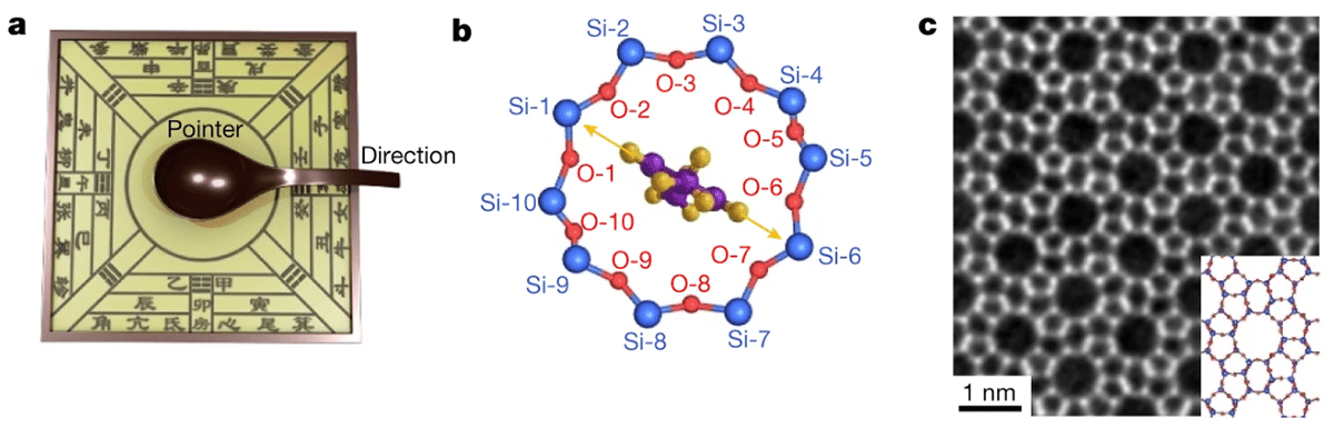
The system in the Tsinghua team’s experiment is very sensitive to electron beams, and is made from single molecules of para-xylene (containing eight carbon and ten oxygen atoms each) trapped within the voids of a zeolite crystal. (Zeolites are microporous minerals that occur naturally but are also produced industrially on a large scale.) The type of zeolite used in this research, known as ZSM-5, consists of rings of silicon and oxygen atoms that link up around large holes in a two-dimensional lattice sheet. When a few of these sheets are stacked on top of one another, the holes align, creating shallow channels through the structure. It was into these channels that Wei and colleagues placed their para-xylene molecules by mixing ZSM-5 powder and para-xylene liquid in a centrifuge.

Figure showing a traditional Chinese compass with schematic and STEM images of the molecular compass

To make their compass, Wei and colleagues took advantage of the fact that the perimeter of each hole consists of a ring of 10 silicon and 10 oxygen atoms interspersed at roughly equal intervals of 18 degrees. The idea was to use the para-xylene molecule inside each ring as a pointer. Because any shift in the molecule’s axis relative to the silicon and oxygen atoms (the “compass points”) would indicate changes in local van der Waals interactions, the researchers could determine the nature of these changes by imaging the molecule and observing the orientation of its long axis in the plane of the ring.

Tiny force changes

Wei and co-workers showed they could indeed use their compass to measure force changes in both space and time. They did this by comparing changes in the orientation of the para-xylene pointers, as seen in the images provided by iDPC-STEM, with variations in the shape of the (slightly elliptical) rings. They gauged these variations by using intensity measurements to establish the distance between pairs of atoms on opposite sides of the rings.

The researchers compared multiple rings and found that the pointers tend to line up along the major axis in each ellipse. They also found that the pointer in any given ring tends to move between compass points so that it stays aligned with the longest axis as the ring changes shape (as a result of increasing exposure to electrons).

To relate these responses to changes in van der Waals interactions, the researchers used first principles calculations to work out how the para-xylene molecules’ interaction energy ought to vary with ring geometry. They found that for each different ellipse, it was always energetically favourable for the molecule to line up along the longest axis – demonstrating, they say, that each molecule in its crystal void does indeed function as a “van der Waals compass”.

Challenges of interpretation

Chen argues that the work could have applications in optimizing zeolite-based catalysis – a process used, among other things, to convert alcohol into petrol. As she points out, ZSM-5 contains aluminium atoms, which can provide protons during the acid-base interactions vital to such catalysis.

Other experts have responded with a mixture of enthusiasm and caution. Shigeki Kawai of the National Institute for Materials Science in Tsukuba, Japan, says that while electron microscopy has already been used to image single molecules, no-one has previously anchored a single molecule inside zeolite pores. This capability, he reckons, might allow two different molecules to be aligned or even reacted with one another.

Bart Kooi of the University of Groningen in the Netherlands, meanwhile, praises Wei and colleagues’ “nicely prepared samples and state-of-the-art imaging”. However, he adds that using two-dimensional images to represent three-dimensional structures complicates the process of calculating the interaction energy. He also questions the extent to which the imaging electrons – even in low doses – might still affect the atomic structures being studied.

The research is published in Nature.

Crisis in a lockdown: how NIST coped with a radiation leak

On the morning of Wednesday 3 February 2021, the research reactor at the National Institute of Standards and Technology (NIST), just outside Washington, DC, was starting to come back online after routine maintenance. Shortly after 9 a.m., however, radiation monitors in the building detected above-normal background radioactivity, consisting of fission fragments from the ruptured cladding of a fuel element. The reactor automatically shut down.

NIST is one of the US’s leading metrology labs, located in Gaithersburg, Maryland, whose 60,000 or so inhabitants may not even know about the presence of a reactor in their midst. Although just half an hour’s drive from the White House, the NIST campus is in an ordinary residential area. However, the reactor’s long-term survival may depend on the local community – and its residents – being able to make a clear and accurate appraisal of its value and safety.

News of accidents at nuclear reactors, wherever they are in the world, often triggers uncertainty, fear and even panic

News of accidents at nuclear reactors, wherever they are in the world, often triggers uncertainty, fear and even panic. Whatever NIST did next to publicize the incident was therefore going to be highly risky for the lab, the reactor and the research community that depends on it. Commenting immediately, before much information was available, might make it appear as though the lab were in the dark. Holding off an announcement pending an investigation would invite accusations of a cover-up, and seem to open the possibility of worse news to follow.

Then and now

The Gaithersburg research reactor was built on farmland in 1967 by what was then known as the US National Bureau of Standards, which was renamed NIST in 1988. Now officially called the NIST Center for Neutron Research (NCNR), it’s used by some 3000 scientists each year and is still vitally important to the US neutron community. Indeed, the NCNR supports about half of all neutron-scattering work in the country. Any interruption in its operation, however brief, would be devastating for neutron research.

But how was NIST to handle the release of information about the incident? The messaging was critical. I immediately recalled how Brookhaven National Laboratory’s High Flux Beam Reactor was forced to shut down permanently in 1999 after tritium-containing water, of no environmental or health impact, leaked from its spent fuel pool. As it transpired, early in the evening on 3 February, NIST put a notice on its website, sent out the news on social media, and asked Gaithersburg city officials to help spread the word.

“We’ve just released a statement on today’s alert at the NIST Center for Neutron Research,” the lab tweeted that evening. “Health and safety of our staff and community is our top priority. No indications of elevated radiation levels outside the building.” This was followed a few minutes later by another tweet: “The ­public remains safe.”

Two days later, NIST posted a 500-word update on its website and via Twitter and Facebook, saying that, after taking a shower, members of staff who had been exposed to the radiation were cleared to go home. It also said that the Nuclear Regulatory Commission (NRC), which licenses and regulates the reactor, had declared the facility and the public safe.

The reactor, NIST reminded the public, had operated safely for 50 years and was a valuable national resource. Its notice also stressed the differences between the NCNR and power reactors, which typically run at more than 100 times the power of research reactors and are much different in size, scale, structure and operation.

A week after the incident, on 10 February, the lab held a virtual public town-hall meeting. Questions were allowed to be submitted by e-mail or via the meeting platform’s Q&A function, and voices and video were muted (questions could be asked anonymously). Around 240 people attended, and NIST’s acting director Jim Olthoff answered all questions. The lab put up the questions and responses on an updateable web page).

A week later, on 18 February, Rob Dimeo, director of NIST’s Center for
Neutron Research, held a virtual town-hall meeting for the neutron-user community. It was attended by around 300 people concerned with how long the reactor would be down, and how its closure would affect their research. Here, too, attendees were muted and questions submitted via e-mail and the platform’s Q&A, as well as by chat.

The virtual format, mandated by the COVID-19 lockdown, meant that the town-hall meetings could be quickly arranged and draw possibly more people than might otherwise have attended

Interestingly, the virtual format, mandated by the COVID-19 lockdown, meant that the meetings could be quickly arranged and draw possibly more people than might otherwise have attended. “The virtual environment allowed for a more measured interaction between NIST and members of the public,” said NRC public affairs officer Scott Burnell. “People were submitting questions via chat, not open mike, which kept the temperature of the room under control.”

But the format was risky, as accepting questions only in writing and muting participants ran the danger of leaving them feeling indulged and patronized, spurring them to seek other forms of venting and information-spreading, which social media famously invites. So did NIST convey an accurate and transparent portrayal of the incident without condescension on the one hand or provoking unnecessary fears on the other? “It’s too early to draw conclusions,” Jennifer Huergo, NIST’s director of media relations, told me. “We did our best with the tools at hand.”

The critical point

Reactors are indispensable scientific instruments, which address national needs and would cost billions of dollars to replace, if indeed any government had the will to try. They are also lightning rods for political and social concerns. The future of neutron research depends not only on building and maintaining more neutron facilities, but also on understanding and addressing the concerns that they arouse. Paying attention to how episodes like the one at NIST play out is a first step.

Copyright © 2026 by IOP Publishing Ltd and individual contributors