The pursuit, exploration and utilization of the space environment can be misinterpreted as a luxury. History portrays space as an exclusive domain for global powers looking to demonstrate their prowess through technological marvels, or the stage for far-off exploration and scientific endeavour with little impact on daily life. However, the benefits of space are already woven into our everyday routines and provide utilities and resources on which the society has grown dependent. If these were suddenly to disappear and the world were to experience just “a day without space”, the consequences would be evident to all.
Our biggest space-based resource is the satellites we’ve put in orbit around the Earth. Communication satellites provide global connectivity and the means to transmit live television around the world. We can remotely watch international events and sporting spectacles in real time, thanks to this space-borne infrastructure. Earth observation is also of growing importance, letting us monitor and assess our natural habitat and climate, which in turn enables us to optimize agricultural land use, to predict and intervene in national disasters, to organize relief efforts, and more besides.
Position, navigation and timing (PNT) satellites provide valuable location data for drivers and outdoor enthusiasts, while their timing signals are also used to timestamp and co-ordinate global cash withdrawals and financial transactions. Satellites provide platforms for science and technology, and they can give universities access to orbital experimentation. Companies are learning to rapidly develop technology through prototypes placed in orbit, while research into space weather using in-orbit instruments provides improved understanding and forecasting to protect our Earth-bound power grids from solar storms.
The utilization of space is set to become more important still. A new vision for the future is starting to emerge that will feature even more innovative uses of space, ranging from space-based manufacturing and energy production to global Internet connectivity. Space-debris management is also receiving greater focus alongside lunar and Martian exploration, and even space tourism.
While some of these new innovations may sound like they are confined to the realm of science fiction, there are already companies furthering the technology to turn them into reality.
Affordable space access
One of the fundamental challenges associated with exploring and working in space is that whatever is up there, starts down here. Escaping Earth’s gravity and achieving orbit is technically difficult, operationally complex and financially exclusive.
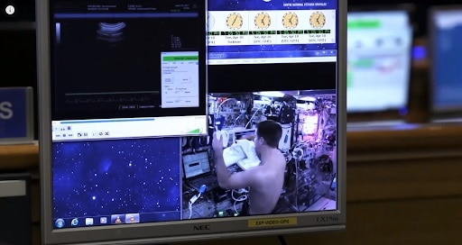
The tide is turning, however, and the world is in the midst of a transformational era in the history of spaceflight. An activity once limited to governments and national space agencies is now witnessing a flourish of innovation led by entrepreneurial private companies such as Rocket Lab, Virgin Orbit and SpaceX, the latter of which was in the global spotlight as watched the US Commercial Crew Programme launched American astronauts to the International Space Station and then return them safely earlier this year. By optimizing conventional rocket technology, these firms are rapidly reducing the cost of space access and generating launch capacity. This in turn is creating opportunities for new space operators and is beginning to initiate a virtuous circle, in which reduced launch costs and increased flight rates create additional commercial opportunities and more demand for launch services. Indeed, the investment bank Morgan Stanley estimates that the global space market will be worth $1 trillion per year by 2040.
The global space-access industry will be limited if it remains focused on optimizing conventional rocket technology, which was first used in the mid-20th century
While this cycle could significantly reduce launch costs even further, it will be limited if the global space-access industry remains focused on optimizing conventional rocket technology, which was first used in the mid-20th century. That’s why we here at Reaction Engines in the UK (see box below) are developing the Synergetic Air Breathing Rocket Engine (SABRE) – what we think will be the next generation of space-propulsion technology. Our aim is to enable horizontally launched reusable space vehicles that are affordable, reliable and responsive, and can be launched at a high and regular frequency.
SABRE versus conventional rockets
Conventional rocket vehicles are propelled by a fuel (liquid hydrogen, kerosene or methane) and an oxidizer (liquid oxygen) carried within the vehicle body. When the fuel and oxidizer combust, mass is projected out of the back of the rocket, creating thrust. However, this approach – and especially the use of heavy on-board liquid oxygen – is constrained by Tsiolkovsky’s rocket equation. It basically tells us that everything carried on board a vehicle has a penalty in the form of the additional propellant, and structural mass of the vehicle, needed to get it off the ground. In other words, this approach hampers mission performance, mission payload and mission time.
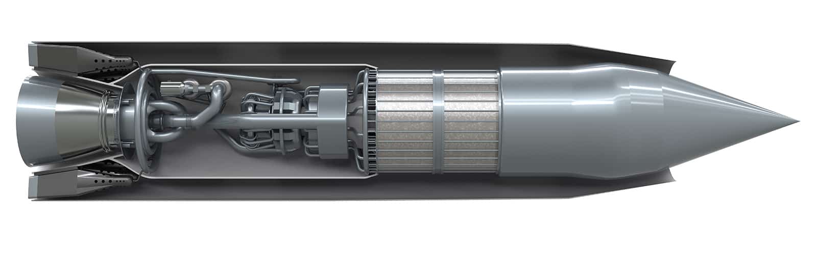
SABRE, on the other hand, is a hybrid air-breathing rocket engine. During the atmospheric segment of its ascent, it will use oxygen from the atmosphere instead of carrying it inside the vehicle, before switching to on-board oxygen upon leaving the atmosphere. A SABRE-powered launch vehicle will therefore have lower mass for a given payload than a conventional rocket vehicle. This mass benefit can be traded for systems that will enable reusability and aircraft-like traits, such as wings, undercarriage and thermal-protection systems – all the features needed to fly the same vehicle over and over again, achieving hundreds of launches.
Reusability will not only drive down the cost of the launch. SABRE-powered launch vehicles will also take off like aircraft instead of launching vertically like conventional rocket vehicles. As a result, they will introduce faster turnaround times, higher vehicle utilization rates and more responsive launches. They will be able to undertake safe abort and return-to-base scenarios. The design of SABRE-powered launch vehicles will also allow more rapid set-up and simpler launch facilities compared with current vehicle designs.
At Reaction Engines, we think these characteristics are far beyond what we see from even the most advanced expendable systems currently available – and that they therefore will unlock the full virtuous cycle for space access and the greater potential of the space economy.
The precooler
The key element within SABRE is its unique, high-performance thermal-management system, which relies on fundamental thermodynamics to extract, redirect and utilize the enthalpy of a hypersonic (Mach 5) airstream as it enters the engine. One of the most important parts of this system is the precooler, which was therefore one of the first pieces of SABRE technology to be developed.
The speed of existing air-breathing engines is limited by their ability to handle and exploit the energy contained within high-Mach air streams. To create thrust from an air-breathing engine you have to increase the speed of the air that passes through it. Counterintuitively, you also have to slow the air down when you reach high speeds so that the internal machinery can apply work into the airflow before accelerating it from the back of the engine.
However, when fast-moving air slows down, it rapidly heats up as kinetic energy is converted into thermal energy. For example, these temperatures can reach over 1000 °C when slowing a Mach 5 air stream. At such high temperatures, it is not possible to maintain the integrity of conventional engine components – quite simply, they melt.

Together, SABRE’s thermal management system and the precooler provide a solution to this problem. When high-Mach air enters SABRE, it is first slowed down by the intake of the engine through a series of shockwaves created by the geometry of the engine’s components. As this happens the air rapidly heats up, but is then passed into the precooler where its temperature is reduced to manageable levels. The precooler has been designed to create heat transfer between the air stream and an internal fluid medium (cryogenic helium). Geometry, fluid properties, and thermal and mechanical effects have all been considered so as to maximize the extraction of heat from the air stream.
With the air stream suitably cooled, it can now enter the heart of the engine, where it goes through a cycle involving compression, combustion, regeneration and, ultimately, expansion through the engine’s nozzle thereby creating propulsive force. The air stream’s thermal energy, which has been transferred to the precooler fluid, is also used to drive the internal components of the engine.
The precooler can cool high mass-flow airstreams from temperatures above 1000 °C to ambient in less than 50 milliseconds, within a compact and low-weight design. It is formed from over 42 km of tubing, the walls of which are thinner than a human hair – thereby providing an enormous area for heat-transfer between the air and cooling medium.
Putting it to the test
In 2012 Reaction Engines manufactured a fully operational precooler and tested it more than 700 times, verifying the ability to take ambient air down to cryogenic temperatures. This prototype unit saw more test time than an already operational prospective SABRE precooler, and performed impeccably throughout.
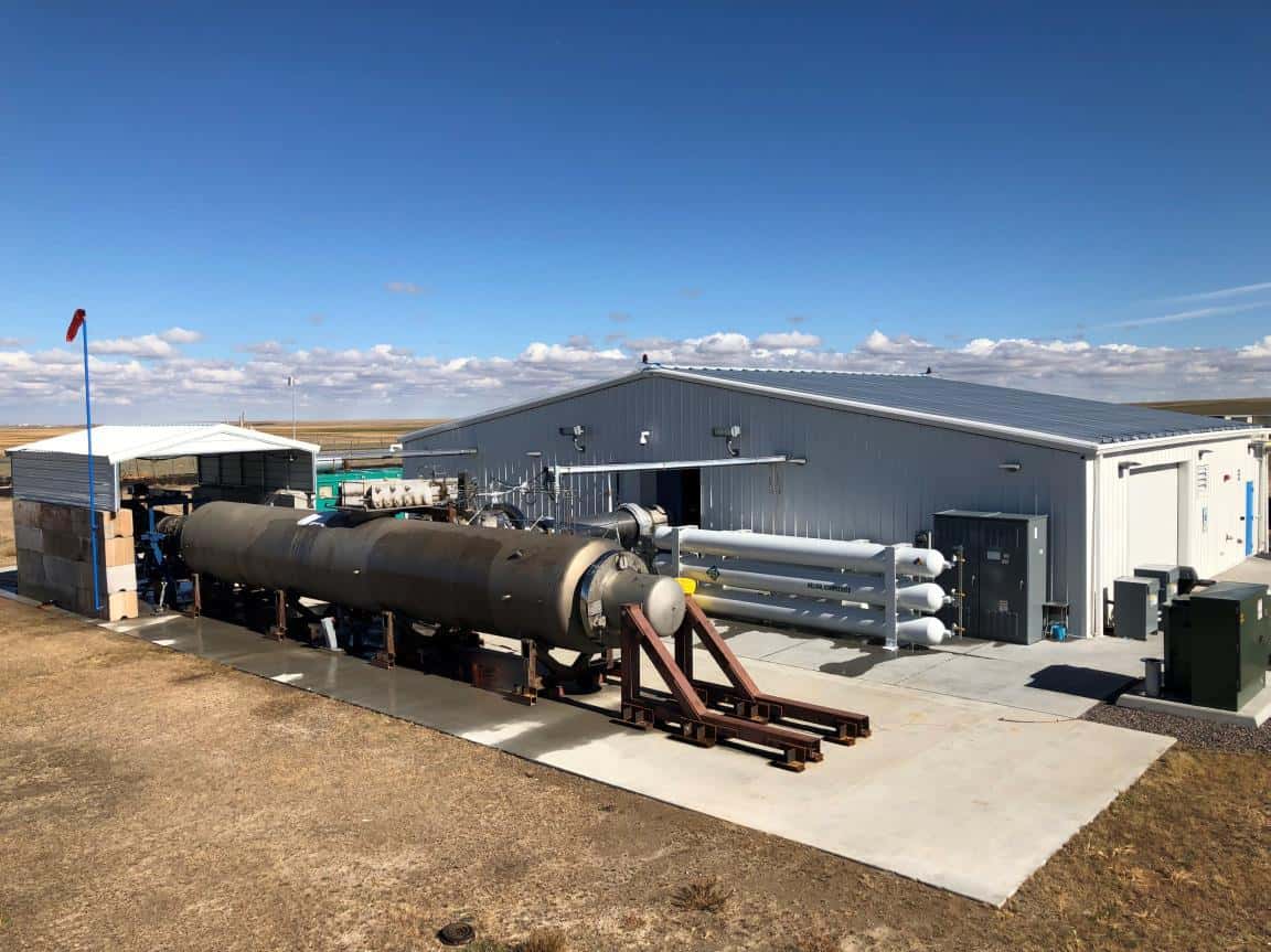
Next came the Hot Heat Exchanger (HTX) test campaign, which was designed to subject the precooler to a range of high-temperature conditions representative of high-Mach flight. Carried out in 2019, the testing took place at a specially constructed facility at the Colorado Air and Space Port near Denver in the US. The test set-up featured a conventional fighter aircraft engine running on full afterburner in order to create the high-mass air flow and high-temperature conditions a SABRE precooler will experience in flight after stagnating (or slowing down) a Mach 5 airstream.
Three hot test campaigns were conducted, with each achieving a higher equivalent Mach number. The final round of tests saw both the precooler and test equipment pushed to their limits, and successfully deliver the ultimate Mach 5 test objective – it demonstrated that the precooler could quench airflow temperatures in excess of 1000 °C in less than 50 milliseconds.
The tests showed the precooler’s ability to successfully cool airflow at speeds much higher than the operational limit of any jet-engine-powered aircraft in history. It ran at over twice the operational conditions of Concorde and over one and a half times the conditions of the SR71 Blackbird. This remarkable precooler technology is, therefore, not only key to the SABRE engine but also offers propulsion solutions for high-Mach and hypersonic aircraft that remain within the atmosphere.
What comes next?
Since the successful HTX test campaign, the next phase of SABRE testing is now under way in its “core engine campaign”, which aims to validate the performance of the air-breathing core. This part of SABRE is responsible for recycling the thermal energy extracted through the precooler into the engine’s internal components. It is also where the incoming air is compressed, mixed with hydrogen fuel and then burnt within the engine’s combustion systems prior to being expanded through its nozzle. This stage will prove the viability of SABRE’s entire thermodynamic cycle and will be a landmark moment when it is demonstrated for the first time.
While the precise timings of this latest phase of the test campaign have been hit by the COVID-19 restrictions imposed in the UK, an extensive design process has already been conducted in conjunction with the UK and European space agencies, which will enable the programme to swiftly progress once the restrictions are reduced. And while the COVID-19 pandemic has undoubtedly impacted both the global aerospace sector and the operation of manufacturing and R&D facilities in the UK, there remains robust demand in the commercial space-launch sector. Reaction Engines can already see a number of possibilities where applications of SABRE-class engines might be used in launch-vehicle architectures, and we are working with partners across the space industry to understand how these capabilities can be brought to the fore.
Technology spinout
Despite being originally conceived as an engine for enabling low-cost space access, it’s now clear that SABRE technology could provide benefits beyond the space industry. That’s why Reaction Engines is also developing spin-out applications of the technology with other industry partners.
In the aerospace sector, SABRE’s thermal-management capability and heat-exchanger technology could boost the efficiency of next-generation commercial aircraft engines and systems, as well as high-Mach and hypersonic aircraft. At a time when the aerospace industry must demonstrate resilience in the face of COVID-19, technological paradigm shifts and challenging decarbonization targets, SABRE technology could help by providing a range of efficiency improvements and cost savings for current and future aircraft concepts.
Reaction Engines is investigating how SABRE technology could benefit other sectors too. Motorsport, industrial processes and the energy industry are all areas where intelligent thermal management, such as that at the heart of SABRE, could bring about significant change. Reaction Engines is keen to adapt and deploy its technology into these industries to make them more efficient, more sustainable, and better for the environment.
It is clear that the space industry is going through a period of significant innovation and rapid development. Innovative new commercial entrants have lowered the cost of space access, which has in turn opened up further commercial opportunities in space.
As the industry develops and the demand for ultra-low-cost access to space increases, we believe that there will be a need for the kind of revolutionary leap forward in propulsion that SABRE and its thermal-management systems represent.
Reaction Engines
Reaction Engines is a UK company founded in 1989 by the propulsion engineers Alan Bond, Richard Varvill and John Scott Scott. They had previously worked together on the RB545 engine, which was destined for use on the Horizontal Takeoff and Landing (HOTOL) system – a space plane concept developed by British Aerospace and Rolls-Royce – in the late 1980s. After HOTOL was cancelled, the team formed Reaction Engines to evolve the HOTOL and RB545 concepts into the SABRE engine class, which the company continues to develop.
After years of fundamental technology development, a UK government grant of £60m in 2015 – coupled with investment from BAE Systems, Rolls-Royce and Boeing HorizonX – has enabled Reaction Engines to grow and transition from research into design and demonstration. Based at the Culham Science Centre in Oxfordshire, the company is working alongside the UK Space Agency, European Space Agency and other organizations in the UK and Europe, to develop SABRE.

 Thibault Brulé is Raman application scientist at HORIBA France, working in the Demonstration Centre at the HORIBA Laboratory in Palaiseau. He is responsible for providing Raman spectroscopy applications support to key customers from various industries, as well as contributing to HORIBA’s application strategies. Prior to joining HORIBA in 2017, he conducted research on proteins in blood characterization based on dynamic surface enhanced Raman spectroscopy. He then applied this technique to cell-secretion monitoring. Thibault holds a MSc from the University of Technologies of Troyes, completed his PhD at the University of Burgundy and followed on with a postdoc fellowship at the University of Montreal.
 Jocelyne Marciano is application scientist at HORIBA France, working in the Demonstration Centre at the HORIBA Laboratory in Palaiseau. She is responsible for testing and demonstrating different types of elemental analysers (EMIA-EMGA, SLFA, MESA and XGT) that are part of the HORIBA Japan product portfolio. Prior to joining HORIBA in 2008, Jocelyne spent 17 years working for Saint-Gobain as a key specialist for glass products analysis. She has in-depth experience in X-ray fluorescence and gas analysers as well as in XPS, SEM-EDX and µ-probe.
 Sharon Hammes-Schiffer received her BA in chemistry from Princeton University in 1988 and her PhD in chemistry from Stanford University in 1993, followed by two years at AT&T Bell Laboratories. She was the Clare Boothe Luce Assistant Professor at the University of Notre Dame from 1995–2000. She then became the Eberly Professor of Biotechnology at The Pennsylvania State University until 2012, when she became the Swanlund Professor of Chemistry at the University of Illinois Urbana-Champaign. Since 2018, she has been the John Gamble Kirkwood Professor of Chemistry at Yale University.