Why ultrafast detection is ultra-good

I once watched a YouTube video that blew my mind. Created in 2011 by Ramesh Raskar and colleagues at the Massachusetts Institute of Technology (MIT) in the US, it showed a pulse of visible laser light less than one-trillionth of a second (10–12 s) long, travelling down an empty, horizontal plastic fizzy-drink bottle (see video below). The light bounced off the inside of the cap, creating a blinding flash as it did so.

Involving millions of repeated measurements, the filming technique was complicated, but it allowed the MIT group to create videos at an effective rate of a trillion frames per second. So although the light took just a billionth of a second (10–9 s) to travel down the bottle, you could see the movement and reflection of the pulse in all its glory. Obviously, to allow the event to be watched properly, the video was shown in super-slow motion, with the light’s journey lasting about 10 seconds when viewed online.

The video was just one of the latest attempts in the quest for “ultrafast photography”, an endeavour that began in 1878 with the recording of a galloping horse and was followed nine years later by the photograph of a bullet moving faster than the speed of sound. Decades later, the development of charge-coupled devices (CCDs) and then complementary metal-oxide-semiconductor (CMOS) technology let researchers study moving objects at rates of up to 107 frames per second. But the 2011 video showed that events could now be captured at a trillion (1012) frames per second.

The big snag with the MIT filming method was that the researchers had to repeat the experiment over and over again, gradually building up their animation of the light. Synchronizing the camera and the laser that generates the pulse – to ensure the timing of every exposure was the same – also needed lots of advanced optical kit and delicate mechanical control. Indeed, it took only a nanosecond for light to scatter through the bottle but an entire hour to collect all the data, prompting Raskar to joke that his system was “the world’s slowest fastest camera”.

However, in 2014 researchers at Washington University in St Louis, US, led by Liang Gao (now at the University of California), developed a way of directly imaging ultrafast events in a single go, rather than having to film them repeatedly. Their technique, dubbed “compressed ultrafast photography”, operates at rates up to 1011 frames per second (Nature 516 74). They used it to take a snapshot of a single photon, which meant they had video recorded the fastest physical entity in the universe (see video below).

Medical magic

With such ultrafast imaging techniques constantly evolving, researchers have naturally wondered about other potential applications, such as studying ultrafast phenomena in biological cells. But could we extend such techniques so they don’t just work with visible light (roughly 1 eV) but detect much higher-energy X-rays (0.1–100 keV) and gamma rays (>100 keV) too? Being able to track such photons with high temporal and spatial resolution would have a massive impact in medical physics.

High-energy photons are already vital in X-ray computed tomography (CT), positron emission tomography (PET) and single photon emission computed tomography. While some of these techniques simply take snapshots of structures within the body (think of a standard X-ray of a broken bone) others look at physiological functions such as blood flow, metabolism and chemical absorption. Being able to detect high-energy photons with higher spatial and temporal resolution would allow us to follow dynamic processes in the body even more closely and continuously.

Take PET, which can measure how fast glucose is consumed around the body, or provide information about blood flow and oxygen use. The technique involves injecting patients with a radioactive tracer, such as fluorine-18. Positrons emitted by the radioisotope collide with electrons in the patient’s tissue, annihilating each other to produce two gamma-ray photons with an energy of 511 keV. Travelling in opposite directions, they’re captured by “scintillator” crystals, triggering the release of lower-energy photons that a photodetector converts into an electric signal.

In revealing the distribution in time and space of the annihilation events, PET therefore indicates roughly where the radioisotope tracer has spread to at a particular time. That information is vital because it tells us how fast the tracer has been able to travel to and from various tissues and organs in the body. PET, in other words, helps us to understand biochemical processes in the body and distinguish between normal and abnormal behaviour.
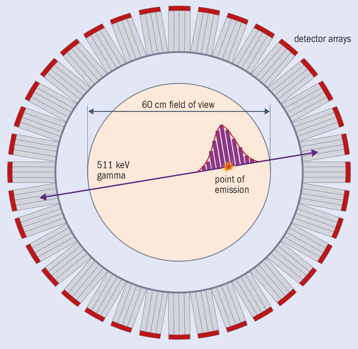
figure 1

Today’s best state-of-the-art clinical PET scanners can achieve a resolution of about 3–4 mm in a scan that lasts a couple of minutes and they offer reasonably good (10%) energy resolution, thereby providing vital information about the biochemical behaviour of the radiotracer in the body. Better images are possible using a new variety of machine known as time-of-flight PET (TOF-PET) scanners, which can measure the tiny time difference between when the two annihilation photons are detected. The world’s current fastest TOF-PET commercial scanner, which is built by Siemens, can resolve processes down to just above 200 picoseconds (200 × 10–12 s) (figure 1).

That kind of timing resolution is excellent and, what’s more, the signal-to-noise ratio is 2.5 times higher than with PET scanners that don’t use timing information. So, if – and it’s a big if – detectors could operate at still faster speeds of, say, 10 ps, we’d get even better maps of where the photons originated. Indeed, the signal-to-noise ratio of the images is expected to rise by a factor of 12 according to a formula developed by Maurizio Conti and colleagues from Siemens in 2013 (IEEE Transactions on Nuclear Science 60 87).

Access all areas

Huge improvements of that kind, brought about by high-resolution, ultrafast gamma-ray detectors, could bring many practical benefits in medicine. Clinicians would be able to examine patients faster, reduce the isotope doses they need, and improve the quality, resolution, accuracy and precision of the images that are so vital for medical diagnoses. But such detectors could benefit many other areas too, which is what prompted the European Union (EU) to fund the Fast Advanced Scintillation Timing (FAST) project.

Led by Etiennette Auffray Hillemanns, a physicist at the CERN particle-physics lab near Geneva, FAST ran from 2014 to 2018. Also known as Action TD1401, this multidisciplinary project (of which I was communications manager) was part of the European Cooperation in Science and Technology (COST). Bringing together hundreds of academics and industrialists from 25 different nations, our aim was to create fast, scintillator-based detectors with sub-100 ps timing precision.

In medical physics, such fast photodectors could help develop TOF-CT scanners (Phys. Med. Biol. 65 085013), Cherenkov imaging and neutron imaging. In biology, they could be vital for high-throughput microscopy, time-gated optical tomography, fast cell sorting, and applications where you want to use very low levels of light so you don’t destroy a live sample. Such detectors could also benefit astronomy by boosting our attempts to image gamma-ray bursts and other cosmic sources of high-energy radiation. Future high-luminosity particle colliders – such as the upgrade to CERN’s Large Hadron Collider – could reap the reward too. At a more everyday level, fast detectors will help in automotive LIDAR (light detection and ranging), which is vital for autonomous, self-driving cars.

With so much potential, members of the FAST project decided to focus on three key areas. The first was to find materials that can produce light more quickly (and given that there are many different types of scintillating crystals, this was a big job). The second was to find ways to transport the light faster through the material to ensure it’s collected more quickly by the photodetector. This is a key issue because the crystal in a PET scanner usually has to be 2–3 cm long to stop enough high-energy photons on their journey to the photodetector and so get a big enough signal. Finally, and most importantly, we wanted to develop ways to detect the scintillation light faster and convert it more quickly into an electric signal, while still measuring the deposited energy of the high-energy photon with good precision.

In reaching this final goal, it’s worth noting that fast detectors have been made possible thanks to solid-state silicon photomultipliers, which have replaced conventional vacuum-based photomultiplier tubes as the best way of recording signals from scintillator crystals in PET scanners. Consisting of thousands of single-photon avalanche diodes (SPADs), silicon photomultipliers have continually smashed their time-resolution records. But as Stefan Gundacker from the University of Milano-Bicocca and colleagues at CERN showed last year (Phys. Med. Biol. 64 055012), if we could read these photomultipliers at high frequency, we’d be able to manipulate the signal from each diode and still extract timing and energy information with high resolution.

The key thing about the PET technique is that it produces many scintillation photons, but they don’t all appear at the same time. Silicon photomultipliers help by lowering the threshold between the signal and electronic noise, thereby letting you measure more accurately when the very first scintillation photons in the crystal are produced – and therefore boost the timing resolution. Indeed, the quest to improve PET and other medical-physics applications is what inspired the early developers of silicon photomultipliers in the first place.

In the case of scintillator crystals made from lutetium oxyorthosilicate doped with cerium and calcium (LSO:Ce:Ca), specially adapted front-end electronics can detect the difference in the arrival time of the two annihilation photons – the so-called “coincidence time resolution” (CTR) – of 98 ps for a 2 cm-thick crystal (the size you typically get in an ordinary PET scanner) and just 58 ps for a 3 mm-thick crystal. Even better, the high-frequency-readout means you can exploit another signal too – Cherenkov light emitted by scintillator electrons that have picked up energy from the 511 keV gamma-ray photons and so started moving at faster than the speed of light in the material. This light gives you a way of “time stamping” the arrival of the very first scintillation photons with high timing precision.
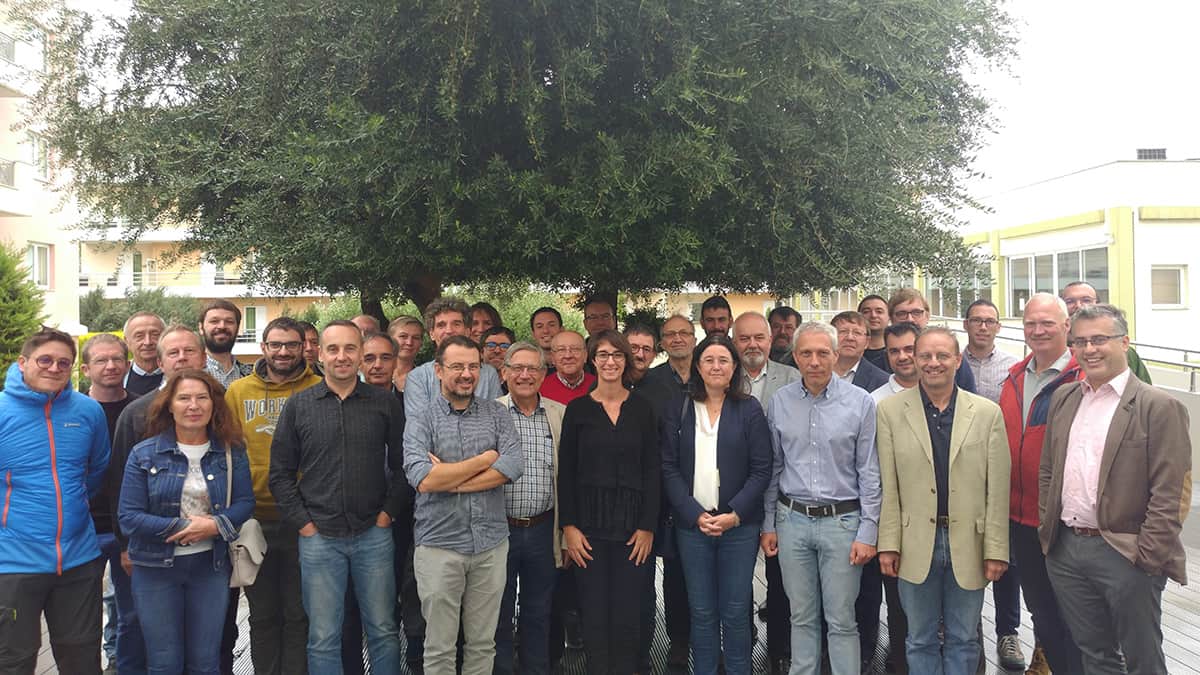
FAST team

For another common PET scintillator – bismuth germatate (Bi4Ge3O12 or BGO) – the CTR was 277 ps for 2 cm-thick crystals and 158 ps for 3 mm crystals. These figures are interesting because although BGO appears slower for PET imaging, it is much cheaper to make than LSO. The other plus-point of BGO is that it’s denser than LSO, which means that a bigger fraction of the incident gamma-ray photons lose all their energy when they interact with the crystal, thereby strengthening the signal. The downside of BGO is that it’s got poor time resolution, so you can’t usually distinguish between events more than a few nanoseconds apart. But with the possibility of extracting timing information using Cherenkov radiation, we might see TOF-PET scanners fitted with BGO crystals at a lower cost.

Another way we could measure photons in PET scanners with a CTR approaching 10 ps would be to use direct-band-gap semiconductors that emit light from excitons (electron–hole pairs). One FAST project, for example, developed a material based on highly luminescent semiconducting nanocrystals made from zinc oxide and gallium embedded in a scintillating polystyrene matrix (Optics Express 24 15289). It emits lots of high-intensity light when the excitons in the polystyrene decay over sub-nanosecond times and then transfer their energy to the nanocrystals, which then scintillate. A second group, meanwhile, showed that a multiple-quantum-well heterostructure based on InGaN/GaN can result in ultrafast luminescence excitation rise and decay times within picoseconds (J. Luminescence 208 119).

Another promising scintillation mechanism for ultrafast timing is known as “hot intraband luminescence”, or IBL (J. Luminescence 198 260). It occurs when a high-energy photon deposits its energy in a scintillator, which within picoseconds spits out a handful of photons over a broad range of energies. Although the IBL yield is far too low for scintillators, it could possibly be combined with other fast-scintillation techniques to time-tag scintillation events and significantly improve time resolution. The IBL yield could also possibly be increased further by engineering the band structure of the material to boost the number and probability of allowed radiative intraband transitions.

In addition to investigating ultrafast scintillation processes, FAST investigated the key parameters for photodetectors and electronics to achieve a good timing resolution. For photodetectors, the photodetection efficiency and the single-photon response are essential to catch the scintillating photons with the fastest timing resolution from the SPADs and provide an electrical signal with the lowest timing jitter. The project also saw researchers develop electronics that could resolve events at picosecond time scales while also ensuring the detector used as little power as possible yet still having a large bandwidth and low noise.

Crystal-clear future
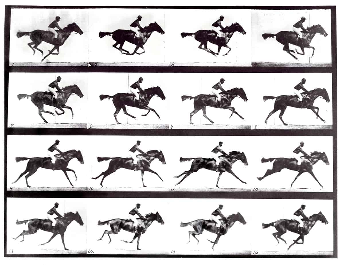
horse gait series of photos

We’ve come a long way from that early 1878 recording of a galloping horse. Indeed, when it came to improving the timing precision of detectors, the FAST project exceeded our expectations. We showed it’s perfectly possible to achieve a CTR of 58 ps and indeed we are now targeting 10 ps timing levels, which would be invaluable in many areas of fundamental and applied science. I believe this objective may be demonstrated in the lab in the foreseeable future, though it’s hard to predict when we’ll see an entire PET scanner built from such fast high-energy photon detectors, let alone become financially viable. Still, I can’t wait to see the first images from an entire-body PET scanner operating with 10 ps CTR detectors (Med. Phys. 10.1002/mp.14122).

The EU FAST project ended in November 2018, but its activities are still alive via the Crystal Clear Collaboration, co-ordinated by researchers at CERN, which played a big role in FAST. Members of the collaboration have already launched a competition, challenging research teams to build the first detector that can resolve events with a time resolution of below 10 ps. Inspired by great historical contests of the past, such as the challenge to find a way to determine longitude at sea, this competition will, I hope, speed up the development of nuclear-instrumentation techniques and applications. And the more teams that join in, the likelier we are to succeed in this grand quest.
Dynamic stimulation of visual cortex lets blind people ‘see’ shapes

A US-based research team has successfully demonstrated how dynamic stimulation of the visual cortex enables blind and sighted people to “see” shapes – a technique that could one day be used to convey entire visual scenes to patients.

Neuroscientists and neurosurgeons have long known that electrical stimulation of electrodes implanted in the visual cortex using small currents produces the perception of a small flash of light, known as a phosphene. This process could serve as the basis for a visual cortical prosthesis (VCP), a device that could restore some visual abilities to blind patients. Although some VCPs were tested in the 1960s and 1970s, they had limited effectiveness and were constrained by the technology of the time. But now a new wave of teams are attempting to produce a modern VCP, using improved electrodes and better wireless data and power transfer technology.

Two such teams, based at Baylor College of Medicine (BCM) and the University of California, Los Angeles (UCLA), have carried out clinical trials and tests of a VCP device called Orion, produced by Second Sight Medical Products. The results, recently published in the journal Cell, show that the Orion device is a safe and effective means of providing patients with some visual experience.

“Our research team is specifically trying to understand how to make the subjects be able to see and discriminate between visual forms such as simple objects or letters. Our key finding is that we can more effectively communicate visual forms to the subject if we use a dynamic electrical stimulation protocol,” says William Bosking, assistant professor of neurosurgery at BCM, who co-wrote the article with senior author Daniel Yoshor, professor of neurosurgery at BCM.

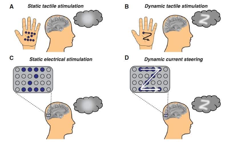
Put simply, this means that instead of treating the electrodes on the array like pixels in a video display, and sending various current levels to all of them at once in an attempt to convey a particular form or shape to the patient, the device instead stimulates only the electrodes that outline the shape it is trying to convey, and stimulates them in a rapid dynamic sequence.

Dynamic stimulation

“This is analogous to how you might trace out a letter on someone’s palm or forearm if you were trying to convey a letter to them by touch,” explains Bosking. “We find that using this dynamic sweeping of activity across the visual cortex allows the subjects to perceive and discriminate letters reliably.”

Visual scenes

The Orion VCP system consists of a camera, which captures an image of the visual scene in front of the patient, a visual processing unit that the subject wears on their belt and which performs some filtering of the camera image, and a transmitter worn on a headset that delivers wireless data and power to a receiving coil implanted under the skin. It also contains circuitry to handle the final conversion of signals into currents to be sent to the electrodes, as well as the electrode array itself, which consists of a flexible sheet with 60 embedded electrodes that lies on the surface of the visual cortex.

“Our research team focuses on understanding how to use the implanted electrodes to produce the best visual experience for the patients. Second Sight is the hardware manufacturer in this case, and we are trying to understand how to best use that hardware to allow the patients to see and discriminate visual forms,” says Bosking.

Bosking notes that with VCPs tested in the past, subjects did not really see or perceive coherent visual forms, instead they tended to see blobs of light in front of them in various locations. “Our new electrical stimulation protocol … produces more coherent perception of visual form, and sends less current to the brain,” he adds.

Looking ahead, the team hopes to test its stimulation protocol in VCPs that have a greater number of implanted electrodes – hundreds to thousands as opposed to the 60 used in the current device. The researchers also want to work with computer vision specialists, engineers and visual neuroscientists to optimize algorithms that could be used to convert a camera image into dynamic stimulation sequences, which could convey entire visual scenes to the patients.

“This would mean continuously updating and identifying each of the salient objects and contours in the scene, and converting these into dynamic sequences that would be delivered to the electrode array in an interlaced fashion,” Bosking explains. “We hope that these techniques will prove useful in future VCPs no matter what type of electrodes or other stimulation technologies are used.”

Bio-bots with spinal cords have natural walking rhythm

A research team from the University of Illinois at Urbana-Champaign has successfully integrated an intact spinal cord with muscle cells to make moving “bio-bots”. The integration of muscle and spinal cord gives the bio-bots’ movement a natural walking rhythm.

Three-dimensional structures that mimic parts of the human body can be used as models to help researchers understand how the actual systems in the body work, or to test new therapies or drugs. Previous versions of bio-bots could move when their muscles contracted. Now, with a spinal cord, the bio-bots can move with a more natural rhythm.

These bots were made for walking

To make the bots, the researchers 3D-printed a small skeleton consisting of two supports and a flexible bridge between them. They then added muscle cells to the skeleton, which grew into a ring of muscle.

One of the more difficult parts of this work was integrating an intact rat’s spinal cord: no one has previously managed to continue to grow an intact rat spinal cord once it had been removed from the animal. After extracting the spinal cord, the researchers added it to the skeleton along with the muscle cells. After one week, they saw that junctions had formed between the spinal cord and muscles. These junctions looked like those formed when neurons connect to muscles in the human body and appeared to show that the spinal cord and muscles were communicating.

To make the muscles contract, the researchers added glutamate to the outside of the bio-bots. Glutamate is a molecule that nerve cells use to send signals to other cells, and adding it to the bio-bots caused their muscle cells to contract in a walking rhythm. Once the glutamate was washed away, the movement stopped.

Taking the next steps

This research marks the first time that a rat spinal cord has been integrated with muscles to make a primitive nervous system. The researchers hope their bio-bots could be used to study the peripheral nervous system – a difficult part of the body to examine in live animals or humans. Their next step will be to improve the bots’ gait to make it resemble a normal walk.

“The development of an in vitro peripheral nervous system – spinal cord, outgrowths and innervated muscle – could allow researchers to study neurodegenerative diseases such as ALS [amyotrophic lateral sclerosis] in real time with greater ease of access to all the impacted components,” says Colin Kaufman, the paper’s lead author. “There are also a variety of ways that this technology could be used as a surgical training tool, from acting as a practice dummy made of real biological tissue to actually helping perform the surgery itself. These applications are, for now, in the fairly distant future, but the inclusion of an intact spinal cord circuit is an important step forward.”

The bio-bot is described in APL Bioengineering.

Microwave timing signals get hundredfold boost in stability

The best-ever conversion of an optical clock’s time signal to a microwave signal has been demonstrated by Takuma Nakamura, Frank Quinlan and colleagues at the National Institute of Standards and Technology (NIST) in the US. The teams achieved the result through a setup involving optical frequency combs and state-of-the-art optical detectors. Their achievement could have significant benefits for fields as wide-ranging as navigation, astronomy, and tests of fundamental physics.

By exploiting the highly stable time signals produced as electrons oscillate between atomic energy levels, today’s optical clocks enable researchers to measure time with unparalleled degrees of accuracy. Indeed, optical clocks produce much better time signals than conventional atomic clocks, which operate at much lower microwave frequencies.

However, optical clocks are difficult to use in most practical timing applications because their optical signals oscillate much too quickly to be counted by electronic devices. To take full advantage of its stability, the optical signal must be converted to an electronics-friendly microwave signal. Two decades ago, the “optical frequency comb” (OFC) was developed to make this conversion.  An OFC produces femtosecond laser pulses with an optical frequency spectrum containing sharp peaks (or tones) that are evenly-spaced in frequency – much like the teeth of a comb.

Frequency gap

Importantly, the frequency gap between these tones is the same as the frequency at which the pulses are emitted by the laser – and this frequency is as stable as the optical time signal itself. When the train of comb pulses is fired at an optical detector, the output is a stable timing signal at a microwave frequency.

While this conversion is straightforward in principle, in practice it has proven very difficult to develop technology that delivers a microwave signal with the desired accuracy and stability. For one thing, the optical detectors themselves can introduce instability to the microwave signal.

Now, Nakamura, Quinlan and colleagues have made an important step forward by improving both their OFC design and optical detectors. The team used signals from two optical clocks as inputs to two independent OFCs that each produced a pulse train. These pulses were sent to two different photodiode detectors to create two independent microwave signals. By comparing these two signals the team concluded  that the microwave timing signals remained in phase with the clocks’ signals to within an error of just 1 in 1018. This makes the signal around 100 times more stable than the current best microwave time sources.

The team envisages numerous possible applications for these stable sources. The ability to maintain stable and accurate microwave signals over large distances would enable more effective synchronization between radio telescope arrays; improvements to radar accuracy; and better communications between satellites. Elsewhere, it could allow for more effective tests of fundamental physics and could even bring about long-awaited improvements to the current SI definition of the second.

The research is described in Science.

Innovation must continue in a COVID-19 world

Can a fusion-reactor design be tested from home? Can your Japanese collaborator understand your mass-spectrometer widget via a shared drawing on a Zoom call? Is an inventor allowed back into their lab to pick up their memory stick? Does your broadband connection work when you need it to? Given the ongoing COVID-19 pandemic, these are just some of the questions now being asked as we encounter a “new normal” in our working lives.

We are in a situation of huge uncertainty. And uncertainty is never great for any business, particularly when it comes to innovation – especially now as most staff are working at home, or at least trying to. Every well-run hi-tech business should ensure that innovation is part of a wider business model, which means that a patent-filing strategy – with its associated cost and time-management – also needs to fit in with that model. If there’s a disconnect here, then there is an increased risk of wasting money, time and effort with little impact.

I work with physicists and engineers from a wide range of entities, including start-ups, spin-outs, universities, small-to-medium enterprises (SMEs) and global corporates. Hard data about what is happening to hi-tech firms is hard to come by. But as a snapshot, there seem to be “pockets” in play, where some are carrying on as if nothing untoward is happening. Some are even increasing innovative activity, while others less so. Physics-based companies arguably lag behind their chemical and biotech counterparts when it comes to protecting and exploiting intellectual property, but the protection of new ideas remains crucial now, just as it did before the COVID-19 pandemic.

From small to large

Before the pandemic, companies had systems and procedures in place to drive, capture and protect innovation. For universities, that might be to help justify tax-payer investment in research and eventually -generate income from spin-outs. For SMEs, a good patent strategy might go hand-in-hand with protecting market share and cementing collaborations. With corporates, the same may be true, but might also form part of a wider “numbers game” where thickets of patent filings could have different tactical use.

It seems that some start-ups and spin-outs are now in a particular bind. Intellectual property might be their main, or perhaps only, asset. If they are lucky to have long-term funding, then day-to-day operations are likely to be okay, for now, and it could even be time to push for more protection. But what if funding was already tight or upcoming funding looks shaky?

This is tricky. Pressing pause can only last so long with patent-office deadlines still looming, even if temporarily extended. It might well be that the protection of certain innovations needs to be ramped down, or jurisdictional coverage restricted. Or perhaps patent rights will have to be abandoned, which would hit the value or strength of the business.

For universities, the risks and rewards in the short term are perhaps not so prevalent. But similar problems do exist. Universities will face financial challenges over the next few years as government funding gets squeezed and international students fall away, which is why many see the protection of innovation as being key to revenue generation. Only time will tell if the short-term pain will justify the possible long-term gain.

For many SMEs, meanwhile, it is common to protect core innovations and also invest in more speculative technology that might be interesting in the future. As a result, such firms might have more options in terms of what to do next. Some will want to push innovation and protection to get ahead of the competition, while others will prefer to pull back and protect their core technology. Both approaches can currently be seen.

For the big corporates, it is quite common for them to follow an “amplified SME” strategy. They tend to carry out more speculative patent filings to protect against future changes in the direction of their sector. In this case, they will likely ride out the storm and more easily cut spending on patents if necessary or cut research investment in more peripheral areas of interest. They may even throw resources behind a particular area of emerging interest. For example, we are seeing an enormous -impetus in the medical-devices sector, in terms of physics-related technology, and also in pharmaceuticals.

The new normal

So what will happen next? Removing more of the uncertainties will bring about increased stability. That might be in terms of more concrete timelines being put in place for a new normal – for example, getting used to working from home or a home–lab combination. Maybe in future researchers will do lab work and then go home and study the data. Perhaps this will now happen, regardless of lockdown measures? Stability is never a bad thing for investors and long-term bets will still be in play.

I still think there will be a shift to an even more electronic and connected world, and there’s clearly going to be a vast amount of innovation to go along with that. Will physics companies be involved in this and benefit from it? Yes. After all, new innovations will still be sought in the telecoms, telemedicine and consumer-electronics industries, as well others too.

We are in a state of huge flux and the world has more to worry about than just physics-based innovation. But if we want a brighter future we cannot simply press pause forever on innovation, protection or exploitation and forget about them entirely. Innovating and protecting your innovation is rarely, if ever, a short-term strategy. It’s long term, critical and needs to fit in with a business model. While the COVID-19 pandemic might change some of the inputs and outputs to the strategy, these messages remain true.

Floating visual displays, ultrafast imaging and far-UVC light: the June 2020 edition of Physics World is now out

Cover of Physics World June 2020 issue

Hovering 3D images are the stuff of science fiction. Just think of R2D2 projecting a message from Princess Leia in Star Wars, or perhaps Iron Man designing his latest tech in Marvel movies.

But in a Faraday cage at the University of Bristol in the UK, fiction is becoming reality with the help of some speakers and polystyrene balls.

As Michael Allen finds out in the cover feature of the June 2020 issue of Physics World, which is now out in print and digital formats, floating visual displays created using acoustically levitated particles could lead to galleries of singing heads, and even to advances in contactless manufacturing.

If you’re a member of the Institute of Physics, you can read the whole of Physics World magazine every month via our digital apps for iOSAndroid and Web browsers. Let us know what you think about the issue on TwitterFacebook or by e-mailing us at pwld@ioppublishing.org.

For the record, here’s a rundown of what else is in the issue.

• US students hit by extra demands – Graduate students under COVID-19 lockdown complain they are being unfairly asked to carry out more tasks such as online teaching, as Peter Gwynne reports

• From “techno-turkey” to iconic observatory – Launched in 1990, the Hubble Space Telescope has almost single-handedly transformed astronomical research and altered the public’s perception of space. Now, three decades on, attention is turning to its successor, as Keith Cooper reports

• From inflation to science policy – Katsuhiko Sato from the University of Tokyo talks to Graham Jones about his work on inflation and the future of physics in Japan

• Shock and awe – How do you react when something unexpected happens in physics? Robert P Crease runs through the gamut of emotions

• Kicking the habit – We all knew that we should have travelled less and video conferenced more. But with COVID-19, we have no other choice says James McKenzie

• Don’t press pause on innovation – Richard Bray says it’s as vital now as it was before the COVID-19 pandemic for physics-based firms to protect their innovation

• The potential of far-UV for the next pandemic – According to the physicist Charlie Ironside, our ability to deal with future deadly pandemics could be better – if we look to the far-ultraviolet. Jon Cartwright reports on a call to arms for the LED industry

• Making images with sound – Floating visual displays created using acoustically levitated particles could lead to galleries of singing heads, and advances in contactless manufacturing. Michael Allen investigates

• Imaginative intersection – Rachel Brazil reviews Entangle: Physics and the Artistic Imagination edited by Ariane Koek

• Explorer versus salesman – Ian Randall reviews Adventures of a Computational Explorer by Stephen Wolfram

• Safe training: the linac simulator – Marco Carlone, founder of Linax Technologies, talks to Tami Freeman about his motivation for  creating an online learning tool that teaches medical physicists how to use and understand linear accelerators

• Ask me anything – Sara Cruddas, space journalist, TV host, author and director

• From the lab to the courtroom – Sidney Perkowitz on crime-solving physicists Wilmer Souder and John H Fisher, who helped further the field of forensics with their research.

Next generation of cryogenics: tailored for quantum technologies

Want to learn more on this subject?

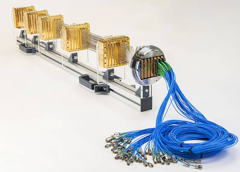
Bluefors webinarIn this Bluefors webinar we will introduce recent developments to support a modern and modular cryogenic measurement infrastructure, which include our XLD side-loader (XLDsl) and new high-density wiring solution.

We will talk about the key enablers for the “second quantum revolution” with the focus on an integrated experimental platform for the control of the quantum degrees of freedom.

In the webinar, Tomi Elovaara, Slawomir Simbierowicz and Joshua Milem will:

  • Present our modular cryogenic infrastructure that enables developments in quantum computing, detector physics, astronomy, materials science and more.
  • Present an integrated platform for cryogenic measurements and show our XLD side-loader system, which enables modularity for both multi-user systems and large experimental efforts.

Want to learn more on this subject?

Left to right: Tomi Elovaara is a sales engineer and member of the sales team at Bluefors. He holds a PhD in condensed matter physics at University of Turku. He joined Bluefors in 2016 as a cryo engineer and has been working in the Bluefors sales team since 2018. Tomi’s focus is on introducing and explaining Bluefors new innovations to our customers. Slawomir Simbierowicz is an electronic device engineer and a member of the R&D team at Bluefors. He has worked in the field of quantum technology and cryogenics for five years. His focus at Bluefors is on our cryogenic measurement infrastructure. Joshua Milem is electronic device engineer and a member of the R&D team at Bluefors. He has worked in the field of quantum technology and cryogenics for three years, previously working on novel topological qubit systems. His focus at Bluefors is on our cryogenic measurement infrastructure.


Topological insulators enter the fourth dimension

Materials known as topological insulators have the unusual property of being able to conduct electricity on their surface even though they are insulators inside. If that weren’t strange enough, physicists have now shown experimentally that such materials can exist in four spatial dimensions. The researchers, based in Singapore and the UK, achieved this feat by wiring up a stack of electric circuit boards to represent a highly interconnected lattice, and say that their scheme could be extended to five or even six dimensions.

The importance of topology can be seen by comparing the spatial characteristics of a sphere and a doughnut. It’s not possible to transform one into the other by gradually varying their shapes – no amount of stretching, squeezing or other distortion will turn a doughnut into a sphere, and vice-versa. Such a change can only come about through an abrupt, discontinuous action – the insertion or removal of a hole.

A similar idea underpins topological insulators, but the transformation in this case doesn’t involve a material’s spatial properties. Instead, it concerns the wavefunctions of the electrons flowing in the material. These contain what is in effect a knot, making it impossible to smoothly convert a topological insulator into a normal insulator. Instead, the material must first become a metal. This means that the material’s physical boundary with the outside world conducts electricity, even though its bulk is insulating.

This phenomenon has previously been seen in two and three dimensions. In the former case, first observed in 2007 and similar to the quantum Hall effect, the material in question consists of an insulating plane with one-dimensional electric currents flowing around the edge. The latter case, detected from 2008 onwards, sees currents flowing in a range of directions across the surfaces of a bulk insulator. In both cases, the currents are generated when an electron’s spin interacts with its orbital motion as it travels through space. These currents persist even when the edges or surfaces involved are deformed.

Beyond three dimensions

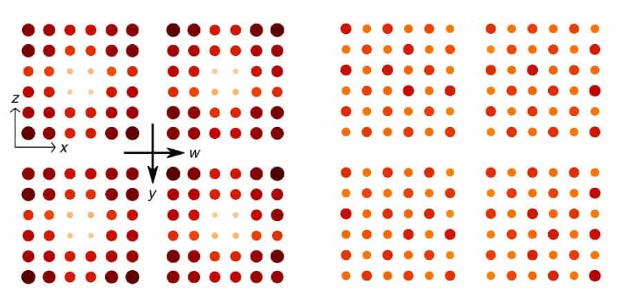
Theorists tell us that topological insulators should also exist in higher dimensions. Indeed, researchers have previously observed them in four dimensions, but they did so by mapping a 4D system to a 2D one. The latest work instead involves the direct creation of a 4D topological insulator that acts as a standard insulator when confined to three or fewer dimensions, and only exhibits its exotic properties once it is extended into the fourth.

The new 4D insulator is based on a model drawn up by Hannah Price of the University of Birmingham, and has been experimentally realized by a team led by Yidong Chong at Nanyang Technological University. To create their insulator, the team relied on an artificial construct known as a metamaterial. Building this metamaterial involved making dozens of electrical oscillators from capacitors and inductors, and then arranging them in grids on several circuit boards stacked on top of one another. With each oscillator behaving like an artificial atom, says Chong, the system as a whole acts like a crystal through which electric current can flow.

Two sets of four square grids of dots. The left set has dark red dots on the edge of the grid, representing high current flow. The right set has milder yellow-to-orange dots throughout, representing low current flow (insulator state)

The idea was to hook up the oscillators so that they behave electrically as they would in four dimensions, even though they are actually sitting in our 3D world. As Chong explains, this wouldn’t be possible if each oscillator were only linked to its nearest neighbours. But an extra dimension can be added to an otherwise one-dimensional row of oscillators by linking each of those objects to two others further up and down the line. This idea can then be extrapolated so that in 3D space connections beyond those to the (six) nearest neighbours yield a circuit that behaves as if it were sitting in 4D-space.

Testing predictions

To test their system, Chong and colleagues sent voltage pulses through the circuits. They found that when the circuits were wired up according to Price’s model those pulses propagated in waves across the connections made to create the material’s 3D “surface” but not within the 4D bulk. They also observed that by tweaking the circuit components they could make the waves disappear from the surface – so turning the material into a straightforward insulator.

According to Chong, scientists had previously thought it impossible to realize such a 4D system experimentally. “It was believed to be just the province of theoretical study,” he says. “The trick here is that we are not using an actual material but a synthetic one.”

Krzysztof Sacha of Jagiellonian University in Poland, who was not involved in the research, reckons that the work bodes well for possible applications of topological insulators, given that the surface states remained intact even though the components had imprecise values of capacitance and inductance. “Such robustness of topological systems to perturbation is very promising from the point of view of future applications where quantum computing is one of the most important candidates,” he says.

Price says that this particular research won’t be applied to quantum computers because the metamaterial used is a purely classical system that can’t support entanglement. But she argues that the work paves the way for other higher-dimensional systems. “There are suggestions that some really cool things could happen in 5D and 6D,” she says.

Chris Hooley of the University of St Andrews in the UK also thinks it unlikely that this particular system will have immediate applications. But he agrees that in the long term, technology could benefit. “The general idea that protected surface states might be of use in quantum computation has been around for a while,” he notes. “And this sort of system gives us some new kinds of protected surface state, so one never knows!”

The research is published in Nature Communications.

High-quality graphene foams are made from organic waste

High-quality graphene foams have been made from the waste gases produced during the high temperature treatment of organic waste. Researchers in China say their pyrolysis-based technique is cheaper and more environmentally friendly than conventional production methods.

The materials are structurally similar to conventionally manufactured graphene foams, say Hong Jiang at the University of Science and Technology of China in Hefei and colleagues. The foams also display similar electrical-transport performance and were able to filter and absorb liquids such as benzene and paraffin, just like other graphene products.

Graphene foams are porous, 3D versions of the 2D sheet of carbon that is conventional graphene. Like other forms of graphene, they are super strong, have a high electron mobility and are great conductors of heat. The foams have a wide range of potential uses, including in energy storage, environmental purification, chemistry and biosensing.

Chemical vapour deposition

Graphene foams are normally produced by chemical vapour deposition. Carbon containing gases, such as methane, and carrier gases are introduced to a heated metal foam substrate – usually nickel or copper. As the gases contact the substrate, they deposit a film of carbon atoms. Once the reaction is complete, the metal is etched away leaving behind a 3D lattice of graphene.

Chemical vapour deposition is expensive and uses large amounts of hydrogen, methane and other gases – which is why Jiang and colleagues set out to produce graphene using the carbon-rich waste gases from bio-refineries that run off organic waste. These facilities heat biomass to 500 °C or more in the absence of oxygen to produce alternatives to crude oil-based products, such as biofuels. This process, known as pyrolysis, has been used for thousands of years to produce charcoal.

The team set up a high-temperature pyrolysis system and produced graphene foams using two different feedstocks: powdered cellulose and powdered lignin – both derived from plants. The powders were pyrolysed at 800 °C and the waste gases filtered to obtain small-molecule gases. These purified gases were then fed into a chemical vapour deposition chamber and deposited on nickel foam.

Various techniques, including Raman spectroscopy and scanning electron microscopy, were used to probe the structure of the graphene foams. “Both products are good quality with no obvious defects,” Jiang told Physics World.

Straw and sawdust

But powdered cellulose and lignin are not the same as biomass waste. To simulate more conventional organic waste, the researchers next fed their system straw and sawdust. The graphene foams produced showed minor drops in quality compared with those from cellulose and lignin. The researchers say, however, that all the foams they made exhibit uniform structures and excellent performance in environmental or energy-storage applications.

Materials rich in lignin, cellulose and hemicellulose would be best for producing 3D graphene foams, Jiang says. But other organic waste could be used. “The quality of 3D graphene foam may be influenced by other elements of biomass waste,” he explains. “For example, nitrogen or sulphur could be doped into the obtained products if feedstocks contain high amounts [of these elements].”

Edward Randviir, a chemist at Manchester Metropolitan University, who was not involved with the research, told Physics World that as graphene production usually relies on fossil fuels or pure graphite, a critical rare material, looking into alternative production methods is a worthwhile pursuit. He adds that the work shows that producing graphene from renewable biomass is “quite clearly feasible”.

Life-cycle analysis

A life-cycle analysis found that producing graphene foams from the pyrolysis of saw dust uses less energy and has a smaller environmental footprint than a conventional chemical vapour deposition process using methane. Biomass-derived foams had a lower impact in 15 out of 18 categories, including global warming and land use.

As well as graphene foams, Jiang’s process also produces bio-oil. The team say that making a high-value product like graphene alongside such biofuels could make improve the economic viability of biomass pyrolysis and support its wider commercialization.

Randviir is not convinced by this, however. While he thinks there is potential in producing graphene from organic waste, he questions whether it can be done on a large scale. And, if it is possible, the economics may change. Graphene is currently expensive because no one has figured out how to produce it on an industrial scale, he explains. If they did, the price would drop, adding less value to the pyrolysis process.

Jiang and his colleagues are now looking to explore the relationship between the yield of graphene foams and bio-oil, and further evaluate the cost and value of their process. They also wish to enlarge the size of the graphene foams and better control the number of graphene layers, Jiang says.

The research is described in Nature Sustainability.

Sourdough tips from Fermilab, anti-5G USB stick does nothing, tracing a message in a bottle

One curious result of the COVID-19 lockdown is an explosion of interest in making sourdough bread. My wife and my eldest daughter are using their skills as a materials scientist and a biochemist respectively to see who can make the best sourdough (top tip from the biochemist, try baking yours in a covered Dutch oven).

So, it is not surprising that physicists are also getting into the act. There is a fantastic article in Symmetry about a sourdough starter at Fermilab that was brought to the accelerator facility in 2017 – when Ryan Mueller arrived from Texas A&M University with a jar of microbes.

As well as giving a bit of sourdough lore, the article has several recipes and some fantastic photos of bread baked by Fermilab staff. It is by Jerald Pinson and called The sourdough starter physics family.

And if that doesn’t sate your appetite, check out The physics of bread by Bob Crease.

Expensive nonsense

The BBC is reporting that trading standards officers in the UK have come to the not-so-surprising conclusion that a £339 USB stick claimed to offer protection from 5G cellular networks is expensive nonsense. They are seeking a court order to take down the website offering the 5GBioShield, which they describe as being no more than a basic USB memory. Never mind that there is no evidence that 5G is harmful in the first place.

The device claims to use a “holographic nano-layer catalyser” to protect against 5G and apparently has been endorsed by a member of the town of Glastonbury’s 5G Advisory Committee. Perhaps the nano-layer catalyser was too small to be spotted by the officers, who probably don’t have access to an electron microscope.

What puzzles me is that surely anyone who believes that 5G signals are harmful would also be wary of USB technology.

Finally, some serious science. Researchers at ETH Zurich and the Massachusetts Institute of Technology have devised a new algorithm that predicts how objects drift on the sea as a result of currents. This could be useful for speeding up search and rescue operations at sea and cleaning up spilled materials. And of course, you could use it to send a message in a bottle to a friend. You can read more in Search and rescue at sea aided by hidden flow structures.


Copyright © 2026 by IOP Publishing Ltd and individual contributors