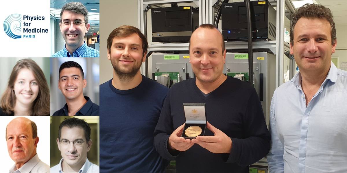
Authors of the award-winning paper (main image, left to right): Clément Papadacci, Mathieu Pernot holding the Rotblat medal and Mickaël Tanter; (insets, top to bottom): Jean Provost, Marion Imbault, Juan Esteban Arango, Mathias Fink and Jean-Luc Gennisson. (Courtesy: Alexandre Dizeux)
A research paper describing an ultrasound imaging technique that can produce ultrafast 3D videos has won its authors the 2019 Physics in Medicine & Biology (PMB) citations prize. This annual prize recognizes the PMB paper that received the most citations in the preceding five years.
The paper, 3D ultrafast ultrasound imaging in vivo, was written by researchers from Physics for Medicine, formerly Institut Langevin (ESPCI ParisTech, CNRS, INSERM and PSL Research University) in France. The winning study, which also won the Roberts Prize for the best paper published in PMB in 2014, describes the first implementation of a novel ultrasound technique that produces 3D videos at thousands of frames per second.
The researchers achieved this high imaging rate by extending their previous work on 2D ultrahigh-frame-rate ultrasound imaging to three dimensions. To do this, they used diverging or plane waves emitted from a sparse virtual array located behind the probe. They designed a customized portable ultrasound system that samples 1024 independent channels and drives a 32×32 matrix-array probe. Graphics processing units were employed to speed the processing of the backscattered signals.
The 3D ultrafast ultrasound system achieved high contrast and resolution. Lead author Mathieu Pernot and colleagues demonstrated its use for several potential applications, including 3D mapping of stiffness and tissue motion, as well as the first real-time imaging of blood flowing through the chambers of a human heart.
Rapid progress
In the years since the paper was published, the field of 3D ultrafast ultrasound imaging has progressed rapidly. Pernot’s team and other groups have used the technique for applications including imaging cardiac blood flow and tissue in the human heart, myocardial fibre imaging, coronary flow imaging and functional brain imaging in animals.
“3D ultrafast imaging remains today a research tool, but the miniaturization of the technology is progressing rapidly and cost-effective solutions are emerging,” says Pernot. “Clinical systems could become available in the next few years.”
As for why the paper attracted so many citations, Pernot suggests that it introduced a transition from ultrasound being perceived as a low-tech imaging modality with high operator dependency to a flexible tool for imaging entire organs with high spatial and temporal resolutions.
“This is a new paradigm for ultrasound imaging,” he says. “3D ultrafast imaging can provide, in quasi-real time, quantitative parameters such as myocardial stiffness or functional connectivity of the brain, which remain challenging to image with other modalities.”
The PMB citations prize is marked with the presentation of the Rotblat medal, named in honour of Sir Joseph Rotblat, PMB’s second and longest-serving editor. “We feel very honoured and proud to receive the Rotblat medal,” Pernot tells Physics World. “Our team, Physics for Medicine, is pursuing the development of new imaging and therapeutic modalities for many years with the support of our institutions and funding organisations such as the ERC and the ANR. The Rotblat Medal is an important recognition of our efforts to achieve these goals at the highest scientific level.”
The winner of the 2019 Physics in Medicine & Biology citations prize is: 3D ultrafast ultrasound imaging in vivo by Jean Provost, Clement Papadacci, Juan Esteban Arango, Marion Imbault, Mathias Fink, Jean-Luc Gennisson, Mickael Tanter and Mathieu Pernot Phys. Med. Biol.59 L1
Researchers in China have fabricated transparent and flexible LED screens using a simple, low-cost manufacturing process based on silver nanowires. Liu Yang and colleagues at Zhejiang University say their technique is an improvement on existing screens, which are too opaque for some applications and can be brittle when deposited on flexible substrates. Their technology could soon bring diverse new capabilities to displays built into the walls and windows of modern buildings.
In recent years, transparent LED screens have become a focus of efforts to make flexible video displays using substrates like glass and clear plastic. Such screens are made from networks of highly transparent conductive circuits that connect their constituent LEDs together. For screens measuring a metre or more, either fluorine-doped tin oxide or indium tin oxide are typically used to construct the circuits. However, networks of this type suffer from several shortcomings, including a complex and expensive manufacturing processes as well as brittleness and a lack of transparency.
In order to design an effective alternative, Yang’s team needed to fabricate a network of wires that was dense enough to distribute electric current throughout the screen, but also sparse enough to preserve transparency. This led them to silver nanowires, which have excellent optical transmittance, electrical conductance, and mechanical flexibility. To manufacture their nanowires, Yang and colleagues first coated plastic and glass substrates with sacrificial masks, etched with networks of straight lines. After treatment in a specialized solution, these lines became stickier than the rest of the substrates. A further spray-coating process led to silver nanowires forming only along these sticky lines, creating an intricate network.
Using this technique, the researchers fabricated a series of 25cm-long, transparent and highly uniform conductive strips from both types of substrate. Through experiments, they showed that these strips possessed both high optical conductivity and low resistance, making them superior to previous tin oxide-based materials. In addition, they demonstrated a screen that hosted a silver nanowire circuit as long as 1.2m; enabling it to emit red, green, and blue light with varying biases, as seen in conventional displays. Finally, they showed that when the circuit was deposited onto a polymer substrate, its performance remained stable even when bent to a radius of 15mm – confirming its flexibility.
Thanks to these advantages, Yang’s team believes their technology could eventually replace tin oxide-based circuits in transparent display applications. The next steps in their research will include developing coatings to protect circuits from the surrounding environment; enhancing substrate adhesion; and sandwiching circuits between substrates for better protection and maintenance. With these improvements in place, the technology shows significant promise in allowing for widespread and practical smart displays.
An illustration of the Berkeley group’s lattice interferometer, where the standing wave of a laser beam in a cavity suspends each atom in a spatially separated quantum superposition state, in the Earth’s gravitational field. (Courtesy: Sarah Davis)
Atoms held in place by laser beams offer a new and more compact means of measuring the local acceleration due to gravity, paving the way for applications ranging from geophysical exploration to sensitive tests of fundamental forces.
The new device, which was developed by Victoria Xuand colleagues at the University of California, Berkeley, US, exploits the quantum properties of cold, trapped atoms to measure tiny variations in the Earth’s gravitational field. Like other such “quantum gravimeters”, it relies on the interference pattern generated when clouds of atoms, or matter waves, are first vertically separated in space, and then allowed to recombine. Because the gravitational acceleration g depends on altitude above the Earth’s surface (as well as factors such as the local density of the Earth’s crust, and the presence of massive objects nearby) the two groups of atoms experience slightly different gravitational potential energies. This difference translates into a phase shift that can be detected in the laboratory.
Suspended in space
The twist is that whereas most gravimeters measure the effects of gravity on atoms as they fall through space, the Berkeley device instead uses atoms that are suspended in an optical trap. This makes it possible for the atoms to interact with the gravitational field for up to 20 seconds, improving the sensitivity of the measurement. “The longer you can allow that phase difference between the two arms of the interferometer to accumulate, the smaller the effect you can measure at the end,” Xu explains. As a result, the team is easily able to measure potential energy differences that arise when atoms are separated by as little as a few microns.
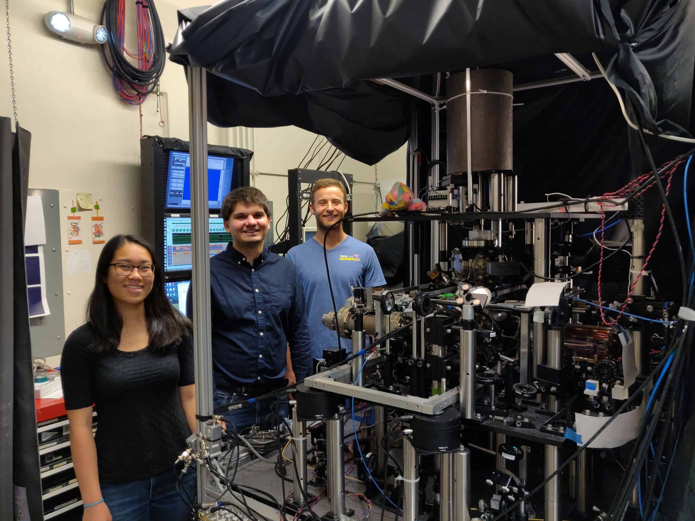
Members of the Berkeley matter-wave interferometry group in the lab. Left-to-right: Victoria Xu, Cristian Panda, Matt Jaffe.(Courtesy: Carter Turnbaugh)
The researchers begin their gravitational measurements by cooling a sample of caesium atoms to 300 nK and launching them upward within a vacuum chamber. Next, they apply a sequence of two pulses of light, set to a frequency and intensity that places the atoms in a quantum superposition of two spatially separated states. At the apex of their trajectory, the atoms are caught in an optical lattice formed by a beam of laser light passing between a pair of highly reflective mirrors. The atoms remain trapped for up to 20 s, at which point the researchers turn off the lattice, allow the atoms to fall, and apply a second pair of light pulses to recombine and interfere the atomic wave packets. The resulting phase difference is proportional to the difference in gravitational potential energy the atoms experienced during their time in the trap.
In addition to its long interaction times, the Berkeley gravimeter has two other advantages over devices based on free-falling atoms. The first is that its geometry makes it far less sensitive to noise caused by vibrations in the laboratory. The second is that it is relatively compact. The team’s entire experimental set-up fits onto an optical bench measuring 1.2 m by 2.4 m, and the atoms themselves move only a few millimetres. An equivalent experiment performed on atoms in free fall would, the researchers note, require a vacuum system half a kilometre tall.
Novel geometry, novel experiments
Xu says that their gravimeter could be used to measure the gravitational potential of small objects. “If you work in a free-fall geometry, this is a pretty hard measurement to do, because you’re just dropping atoms past the signal you’re interested in,” she says. With trapped atoms, in contrast, the atoms can be held in the area where the gradient of the gravitational potential is greatest. This, she says, should make it possible to perform more sensitive measurements of short-range forces, which could be used to test theories of dark energy.
Holger Müller, who leads the Berkeley group, points out that being able to hold atoms in a quantum state for long periods of time could also have applications in other areas of physics. “What we are doing is using quantum mechanics for a useful purpose,” he explains. In their current set-up, the “useful purpose” is measuring tiny variations in the force of gravity, but similar techniques could also be applied to experiments on quantum computation. In either case, Müller adds, the time required to make the measurement is important, but so is the length of time that the atoms remain in a quantum superposition. “What we are doing is vastly extending this second time scale,” he concludes.
This episode of the Physics World Weekly podcast goes to the movies as we discuss how physics and physicists have shaped the film industry – both on and off screen.
Physics World editors chat about wormholes, both real and fictional, and make the case for our favourite science moments in films. We look at how the laws of physics are put to work in visual effects to ensure that everything from weightlessness to curly hair looks realistic on screen. We also chat about what moviemakers and physicists can learn from each other and the science of science fiction.
Finally, we play a physics-and-film related parlour game that is sure to liven-up your next party.
Single-use plastic products could have a more useful and less polluting future thanks to a new technique that “upcycles” them into valuable lubricants and waxes. The technique, known as catalytic hydrogenolysis, uses platinum nanoparticles supported on tiny cubes of strontium titanate perovskite material to convert energy-rich polyethylene molecules into liquid hydrocarbons. The high-quality nature of these hydrocarbons means they could be employed in consumer products, potentially reducing plastic pollution in the environment.
Polyolefins such as polyethylene are widely used in single-use plastic products because the starting materials to make them are cheap and abundant. While these products are vital in some applications – sterile packaging for foods or medical devices, for example – they are being produced in ever-increasing amounts. Around 380 Mt of plastic materials are created worldwide each year, corresponding to roughly 7% of all crude oil and natural gas produced, and some analysts predict that plastic production could quadruple by 2050.
Of these materials, 75% are discarded after just a single use. Most single-use plastic waste ends up in landfills, in the environment, or in incinerators that produce greenhouse gases and toxic by-products as well as electricity. The plastic left in the environment does not easily degrade because of the very strong carbon-carbon bonds present, but instead breaks down into microplastic particles. In instances where it is recycled, current methods tend to produce lower-value materials with degraded properties – a phenomenon known as “downcycling”.
A vast and as-yet untapped resource
Despite this, some scientists view polyolefin waste as a vast and untapped resource for producing higher-grade chemicals and new materials. According to a US-based team led by Kenneth Poeppelmeier at Northwestern University, Aaron Sadow at Ames Lab and Iowa State University and Massimiliano Delferro at Argonne National Laboratory, a more efficient technology for extracting value from discarded polymers could save the equivalent of up to 3.5 billion barrels of crude oil each year. Selective catalytic processes that upcycle plastic waste into valuable products are thus sorely needed.
The researchers have now developed such a process. In their work, the researchers were able to react some of the strong C-C bonds of high-molecular-weight polyethylene with hydrogen converting the material into high-quality liquid hydrocarbons with a lower molecular weight and narrow distribution of between 200 to 1000 Da. Such liquids could be used as lubricating oils or as intermediates such as waxes that can be further processed into ingredients for everyday necessities such as detergents and cosmetics, say the researchers.
The catalyst they used consists of platinum nanoparticles just 2 nm in size deposited onto strontium titanate (SrTiO3) perovskite nanocubes (50-60 nm across) using a technique called atomic layer deposition. This technique, which was developed at Argonne National Laboratory, allows for precise control of the nanocubes. The researchers chose these materials because they are stable at high temperatures and pressures.
The catalyst cleaves the C-C bonds in the PE under moderate pressures of 170 psi H2 and temperatures of 300°C. The technique, detailed in ACS Central Science, also produces far less waste than conventional recycling methods, according to Poeppelmeier and colleagues.
Physicists from across Europe have revealed plans for a huge underground gravitational-wave observatory that, if funded, could be operational by the mid-2030s. The European Laboratory for Gravitational and Atom-interferometric Research (ELGAR) could be located in either France or Italy and would cost around €200m to build. Those involved in the project have now applied for European funding to carry out a detailed design and costing for the facility.
Gravitational waves are ripples in space-time that were predicted over 100 years ago by Albert Einstein. In 2015 the twin Advanced Laser Interferometer Gravitational-wave Observatory (aLIGO) in the US along with the Virgo gravitational-wave detector in Italy detected the first gravitational-wave signal and since then tens of such events have been spotted. The observation and pinpointing of such gravitational waves is expected to be boosted in the coming years by the recent completion of Japan’s KAGRA observatory, which is the world’s first underground gravitational-wave observatory to use cryogenic mirrors.
ELGAR is the first large-scale instrument that relies solely on quantum technologies and the only project of research infrastructure in Europe based on matter-wave interferometry
Benjamin Canuel
Rather than detecting gravitational waves by bouncing laser beams off mirrors as carried out by aLIGO, Virgo and KAGRA, ELGAR would instead use atom interferometry. This involves splitting an atom beam – rubidium atoms in ELGAR’s case — in half and allowing both halves to travel for a certain distance before being recombined to look for differences in their paths. A slightly longer path would result from a tiny curvature in space-time that could be caused by a passing gravitational wave.
Atom interferometers tend to be more sensitive at low frequency than their laser counterparts as atomic beams travel more slowly. “The technology for ELGAR is already mature,” says Benjamin Canuel from the Photonics, Numerial and Nanosciences Laboratory (LP2N) at the Institut d’Optique Graduate School in Bordeaux, who is coordinating the ELGAR proposal. “Many technological bricks of the ELGAR detector are now available in lab experiments but an ambitious R&D programme is required to benefit from those techniques in a large research infrastructure.”
Plugging the gap
ELGAR would feature two 32 km long arms that each would contain 80 atom “gradiometers” that are separated by 200 m. The gradiometers would measure the relative difference in the positions of the atoms beams as they pass through. This set-up would allow researchers to detect gravitational waves in the 0.1–10 Hz frequency range, which would be emitted, for example, by medium-size black-hole binaries. These black holes have masses between 100 and one million solar masses and are elusive but crucial to explain whether supermassive black holes formed from the expansion of small black holes, from the merger of multiple smaller black holes, or possibly from other scenarios.
This frequency range would allow researchers to plug a gap in observations given that ground-based detectors like LIGO cover the frequency range from around 10 Hz to 10 000 Hz while the LISA space-based observatory, would, if launched in the 2030s, study gravitational waves between 0.1 mHz to 0.1 Hz.
Three possible sites that have been picked for ELGAR – the Laboratoire Souterrain à Bas Bruit (LSBB) in southern France and two former mines in the Mediterranean island of Sardinia. The LSBB is currently the location for the €12m Matter–wave laser Interferometric Gravitation Antenna (MIGA) — a demonstrator atom interferometer being built by a consortium of 17 French institutions and featuring a 150 m-long optical cavity. MIGA will carry out precision measurements of gravity as well as applications in geosciences and fundamental physics.
“The choice of ELGAR’s location will be another important goal of the design study that should give a precise methodology for site comparison and characterization, and could also eventually consider other sites in Europe,” Canuel told Physics World.
The ELGAR proposal is similar to one announced earlier this year by physicists in China. Known as the Zhaoshan Long-baseline Atom Interferometer Gravitation Antenna – Gravitational Waves (ZAIGA-GW), their facility, if built, would consist of three 1 km-long tunnels in the shape of an equilateral triangle with each arm being an independent atom interferometer. Costing 1.5 billion yuan, it would aim to detect gravitational waves in the 0.1–10 Hz frequency range and could be later upgraded to 3 or 10 km arms.
The team behind the ELGAR proposal come from six European Union countries and they are now applying for funding to carry out a complete design study for the facility including a full cost analysis. “ELGAR is quite unique in Europe,” adds Canuel. “It is the first large-scale instrument that relies solely on quantum technologies and the only project of research infrastructure in Europe based on matter-wave interferometry.”
Of all the subjects that were available to study at school, physics was the one that most appealed to my experimental instincts. I’m not a spectacularly good mathematician. I’m more of an engineer, and I like mucking about with stuff – I like building things and designing things and seeing what happens when you try them out. You get some of that in design and technology courses, too, but school-level physics is very experimental, because most of the mathematical bits end up being taught in the mathematics course as applied maths. So when I went to the University of Cambridge in the 1990s, I started out in physics even though, looking back, I think I had more of a natural affinity for engineering.
In my first year at Cambridge, the course was around 25% computer science, 25% physics, 25% materials science and 25% maths for physics. I enjoyed the experimental parts of the course, and especially the weekly sessions at the Cavendish lab. But the second year was two lots of physics, plus maths for physics, and after that it became clear that I was an engineer more than I was a physicist, so I moved across to engineering.
Why did you decide to go into computer science for your postgraduate work?
I’d been a computer programmer since I was a kid and, on some level, the Raspberry Pi is an attempt to recreate the positive aspects of how people like me learned computing back in the 1980s. I had a BBC Micro computer at school and at home, and a Commodore Amiga at home as well, so I had access to all these programmable machines starting from when I was about 10.
In my postgraduate work, I drifted into working purely on software, designing compilers and programming tools, but I probably went too far in the abstract direction. The place where I’ve ended up is closer to silicon engineering or electrical engineering. The former is kind of a software job these days, now that human beings aren’t drawing polygons that turn into bits of masks on silicon chips anymore. Instead, they’re writing descriptions of the chip’s behaviour in high-level languages and leaving the rest up to the tools they’ve developed. But there’s also an aspect of hands-on work in what I do – the actual grungy bit of getting a PCB [printed circuit board] and stapling stuff down on it to make a physical product you can sell. After a period of oscillation, I guess I ended up somewhere that’s right for me.
How (if at all) has your training in physics helped you in your career?
The maths has been very useful, and the analytical skills have been useful as well for the engineering end of things – basic experimental design, for example. We built the Raspberry Pi 4 recently, and after we put it out “into the wild” we got a lot of data coming in from users on their experiences, saying that this thing is surprisingly fast, or this other feature is surprisingly slow. We like to think that we design our products analytically, but even a small and relatively simple computer like the Raspberry Pi is complicated enough that after you build it, it becomes its own little system, with its own physics. To understand its performance, you need to design experiments to probe its behaviour, and that’s something I took away from my experience with physics.
Read more about Eben Upton’s work and applications of small computers to the industrial “Internet of Things” in this month’s Physics World Focus on Computing
The Internet of Things (IoT) means different things to different people. What’s your definition?
I think we’ve been done a bit of a disservice, because the earliest examples of IoT devices – the ones that people often think about when they hear the term “Internet of Things” – were consumer items such as the Internet-connected light bulbs, smart switches and thermostats made by a company called Nest. I have a Nest myself, but it’s misleading to think of the IoT in terms of stuff like that. Most of the potential for connected devices is on the industrial side, because there, the applications are not limited by human attention.
The number of IoT objects you will have in your life as a consumer is going to be countable on the fingers of one hand. You might have a smart thermostat. You might have a digital assistant-type object like Amazon’s Alexa. You might have some home automation to turn lights on and off and open your garage door. But fundamentally, you only have so much time to interact with connected objects. The industrial IoT is more interesting because it’s largely about machines talking to other machines, and there is no limit to the size of that market as long as there’s a return on investment.
The market for industrial IoT objects is big because of the amount of money you can save. The inefficiencies that abound in, say, manufacturing are so enormous and so demonstrable that you can put in lots of extra automation and monitoring equipment and it will quickly have a large and demonstrable payoff. So, for me, the IoT is much more about factories and making industrial processes run more smoothly than it is about consumer products.
What kind of industrial processes?
I’ll give you an example from the factory that makes Raspberry Pis. The factory is in South Wales and it’s absolutely vast; it’s owned by Sony and they make many other things there as well. The industrial equipment they use tends to have data ports on the back, usually Ethernet ports or serial ports, which spew out data about how the machines are performing – but almost always, historically, nobody’s been listening.
The reason is that to listen properly, you need something to connect to those data ports and do some pre-processing on the data. Then you need to shoot the processed data back over the network to a machine that can store it until you’re ready to analyse it. But until recently, there hasn’t been anything cheap, low-power and compact enough to plug into the data ports, and there’s been nowhere to store the resulting datasets if you wanted to back them up. We’ve also lacked the algorithmic expertise necessary to extract data and turn it into information that would generate insights on how you can improve the performance of the machines.
Now, with the collapse in the cost of data storage, the rise of machine-learning techniques and the emergence of small computers like the Raspberry Pi, that’s all changed. You’ve got a thing you can plug into a piece of industrial equipment to capture that stream of data. You’ve got somewhere to put the data you capture. And once you’ve got it back over the network, you’ve got the tools you need to get information out of it. So what Sony has done is to put in a whole new layer of monitoring to observe the behaviour of the equipment and feed it into “big data” analytics operations – and it’s been done without disrupting the existing industrial control systems the firm has been using for years.
How else could small devices be used?
There are lots of examples, but one of my favourites is that someone put a Raspberry Pi attached to a microphone in their elevator and recorded the sound of the elevator running. Once they’d accumulated enough data, they were able to identify which sounds were bad, in the sense of predicting that the elevator would need maintenance in the near future. The bulk of Raspberry Pi deployments in industry are like that, in the sense that they involve monitoring rather than control, although that’s starting to change.
What makes small computers like the Raspberry Pi suited to these “machines talking to machines” applications?
Low cost and hackability are both important, because together, they reduce the cost of experimentation. We want people to be able to try this stuff, adding monitoring and automation to their production lines, using whatever discretionary budgets they have available to them, without getting locked into a particular vendor. That way they can experiment quickly, and if they get a negative outcome, well, that’s fine, they’ve only spent £50 on a Raspberry Pi. But if they get a positive outcome, the low unit costs of these computers enable them to scale up while maintaining a good return on investment (ROI). The payoffs in some industries are quite large, but you can still win a lot more ROI calculations with a £50 product than you can with a £500 product, which is where we used to be in terms of diagnostic equipment.
There’s also a secondary aspect to ROI calculations, which is the total cost of ownership. If you plug in a PC and leave it idling, it’ll consume tens of pounds’ worth of electricity a year. With a small computer like the Raspberry Pi, that drops to a handful of pounds, and over the years, the difference adds up. The lack of moving parts in a Raspberry Pi also makes it robust, so you don’t have to replace them as often. Building a robust machine was key for us because we were expecting kids to use them, and the metrics we used for that are useful for industry, too. Which is the tougher environment for a computer: an oil rig or a kid’s bedroom?
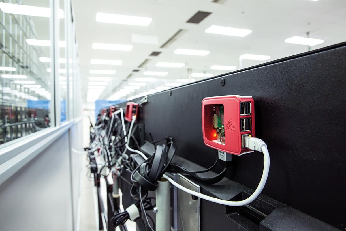
Live data Raspberry Pis act as monitoring systems at the Sony factory in South Wales where they are manufactured. (Courtesy: Raspberry Pi Trading)
Security is another topic that often comes up in conversations about the IoT. How do you keep these machine-to-machine conversations secure?
Whenever you talk about a glorious “big data” universe in which devices are hoovering up large amounts of data, people get queasy about it. That’s not unreasonable. Someone made an IoT television a few years ago that turned out to be recording basically everything that went on in your house and shipping it to the data “cloud”, and people were rightly terrified.
I don’t have an Alexa-type device in my house. I talk about too much secret stuff; my wife works at Raspberry Pi, too, so we talk about the business a lot. But the same problem also surfaces in an industrial context, and I see local data processing as part of the solution. If you’re running a machine-learning-type application, you’re probably not going to be able to train your algorithms locally. But once you’ve got a pre-trained model, you can probably do local inference using the processor on a Raspberry Pi. You can imagine building a monitoring system composed of some cheap sensors connected via Bluetooth to a Raspberry Pi that aggregates data from these sensors, does some processing, and then sends a relatively small amount of relevant data over the network.
For much of the history of computing, progress has been about making faster, more powerful computers. Is that emphasis changing and, if so, what does that tell us about the future direction of the field?
I think the era of free returns in processor speeds is drawing to a close, because we’re running out of atoms. The smallest structures on silicon chips are now spaced around 7 nm apart, which is about 70 atoms, and at those distances both the physics and the economics of the system start to go awry. Our knowledge of the behaviour of semiconductors is based on a statistical model of each thousand silicon atoms having, on average, this many dopant atoms embedded within them. But of course, once you’re making silicon structures 70 atoms apart, it’s no longer a statistical process, so your assumptions start to break down on the physics side. At the same time, on the economic side, it’s becoming ruinously expensive to build faster chips.
Does that mean that Moore’s law no longer holds?
Moore’s law was only ever really an agreement between interested parties – chip designers, foundries and manufacturers of foundry equipment – that the number of transistors per unit area of silicon would advance along an exponential curve at a certain rate. It was kind of a consensus. But the trends that enabled that consensus are coming to an end, and that means we’re beginning to see a new focus on efficiency in software engineering. I’m excited by this because I’m still a software engineer at heart, and until recently it’s been very hard to argue for writing more efficient code because the doubling in computer power meant it wasn’t necessary. You just waited two years, and your code ran twice as fast.
Any other changes?
I’m seeing an increasing focus on communications, making it easier for computers to interact with the real world. There isn’t so much excitement anymore in doing lots and lots of maths really fast on one computer in isolation, and we actually see this on the educational side of our business.
When we built the first Raspberry Pi, I didn’t want to put input-output pins on it, because I thought kids would be interested in using them to write programs. Of course, what children actually love doing with Raspberry Pi is interacting with the real world, building weather stations and robot controllers and things like that. And maybe that was a harbinger of things to come, or the kids were attuned to the zeitgeist more than we were. The kinds of things they were interested in then are the things we’re all interested in now, which is working out what problems computers can solve for you. And now that the era of free returns is coming to an end, I think we can broaden that question out a little bit.
Eben Upton is the co-founder of the Raspberry Pi Foundation and chief executive of its commercial arm, Raspberry Pi Trading, e-mail eben@raspberrypi.org
Read more about Eben Upton and how physics has influenced his work in his “Once a physicist” interview (Physics World, November 2019 p61).
Hollywood often takes a creative licence with the laws of physics. Clearly, there is more to good storytelling than obsessing about accurate science, and part of the fun of going to the cinema is suspending disbelief for a couple of hours. But to create extraordinary – yet believable – worlds on screen, physicists can help filmmakers in a number of ways. Watch this short video to find out how.
‘Physics at the movies’ is the theme of the November special issue of Physics World. The star-studded issue includes exclusive interviews with actors Benedict Cumberbatch and Daniel Radcliffe, who discuss what it’s like to play famous scientists and to work with visual effects teams. Elsewhere in the issue, you can find out about the role of science advisers in Hollywood, how physics is increasingly being hard-wired into computer-generated imagery (CGI), and much more.
Find the full run-down of the November special issue and how you can access it, in this article by Physics World editor Matin Durrani.