Optical frequency comb fits in your back pocket

Physicists in Russia and Switzerland have built the smallest optical frequency comb to date, fitting the entire device into a volume of just 1 cm³. Their research is a significant step towards cheap, easily-produced microcombs – which would be suitable for applications including information processing and telecommunications.

An optical frequency comb is a laser that produces a spectrum of discrete, equally-spaced frequency lines – resembling teeth in a comb. In recent years, they have played important roles in metrology, spectroscopy and communications.

One of the most successful methods for creating the combs’ signature spectra is to couple a continuous wave laser to a microresonator waveguide. These microresonators are ideal for producing the so-called “dissipative Kerr Soliton states” – waves that retain their shapes as they travel. This method, however, still has high loss rates, driving up the power requirements of the devices. This means the driving lasers are large and expensive; making low-cost, portable frequency combs unfeasible.

Minimizing losses

Now, a team led by Tobias Kippenberg at the Swiss Federal Institute of Technology Lausanne has found a way to get around this problem. The team used a highly-sophisticated deposition process to fabricate an ultralow-loss silicon nitride microresonator. They then coupled the microresonator to a chip-based indium phosphide laser diode – a compact device that is widely available commercially.

Intrinsic scattering from the microresonator waveguide reflects a small portion of the laser light back to the laser. This feedback helps to stabilize the laser, eliminating any need for bulky on-chip tuning mechanisms such as electronics and heaters.

Occupying 1 cm³, the team’s frequency comb is the smallest ever produced; allowing it to be integrated onto a single chip and controlled electrically. This was mostly possible because the optical losses sustained by the device’s integrated silicon nitride waveguide were unprecedentedly low, meaning power thresholds were low enough to excite dissipative Kerr soliton states. The device consumes less than 1 W and the spacing between the comb’s teeth is less than 100 GHz.

Kippenberg and his colleagues are confident that such a device could allow for next-generation applications including precise distance measurements using LIDAR, as well as facilitating extremely fast information processing in data centres.

Full results are published in Nature Communications.

Robert Myers named as new director of the Perimeter Institute for Theoretical Physics

The Canadian theoretical physicist Robert Myers has today been unveiled as the next director of one of the world’s leading theoretical physics centres. Myers, 60, takes over from Neil Turok as head of the Perimeter Institute for Theoretical Physics (PI) in Waterloo, Ontario. Turok steps down after a decade leading the Canadian centre to spend more time doing research at the PI.

The PI focuses on fundamental questions in nine areas of physics including cosmology, condensed-matter physics, particle physics and quantum information. Home to more than 150 resident researchers as well as 1000 visiting scholars, the PI was founded in 1999 by Mike Lazaridis, the founder of Research in Motion — the company that made the Blackberry wireless handheld devices.

Perimeter is fortunate to have a respected, dedicated scientist and likeable person like Myers as its new director

Donna Strickland

Founded in 1999, the PI’s research programme began in 2001 with nine scientific staff, soon expanding to 24 by the end of the year. In 2004, the institute moved into its now iconic premises but the PI’s first executive director Howard Burton left suddenly in June 2007 apparently after negotiations over a new contract broke down. A year later, the institute appointed the cosmologist Neil Turok, who was then at Cambridge University, as director — a position he has held for over a decade before announcing  last year that he was going to step down.

Under Turok’s stewardship, the PI continued to expand. In September 2011, it opened the Stephen Hawking Centre, which doubled the size of the institute and provided a space for its Masters students. In 2017, the institute opened its Center for the Universe, which brings together researchers to deal with the huge influx of data emerging from major telescopes such as the Canadian Hydrogen Intensity Mapping Experiment (CHIME) and the Event Horizon Telescope (EHT).

The next phase

Myers’ areas of expertise include black holes, string theory and quantum entanglement. He received his PhD at Princeton University in 1986 and, after a stint at the Kavli Institute for Theoretical Physics at the University of California, Santa Barbara, moved in 1989 to McGill University before joining the PI in 2001. Along with the directorship, Myers will hold the BMO Financial Group Isaac Newton Chair in Theoretical Physics – a position that is supported by a C$4m endowment fund by BMO Financial Group that was made in 2011.

The Perimeter Institute is not just an institute, but a family

Robert Myers

“[Myers] is the perfect choice to lead Perimeter into the future,” says Turok, who will now lead the PI’s Center for the Universe. “He has been my closest advisor throughout my time as director and I am delighted to remain at Perimeter as a researcher with him charting the course for the institute.”

According to Lazaridis, Myers is highly respected throughout the global physics community. “We are thrilled to move into the next exciting phase of Perimeter’s evolution under Myers’ leadership,” adds Lazaridis. “He possesses the drive and vision to advance Perimeter at a particularly exciting time in the history of the Institute and of physics more generally.”

Myers already has some experience leading the PI, having served as interim director for a year following Burton’s exit and been the PI’s interim director since 1 January after Turok stepped down. “I am delighted to have the job,” Myers told Physics World. “It’s a really exciting time and I am looking forward to leading the institute.”

Myers pays tribute to Turok, who he says took the PI to the “next level”, had great ideas and a “keen eye for talent”. But given the recent expansion of the PI into new areas of research, particularly condensed-matter physics, Myers says that initially he will focus on consolidating those areas given that some are small groups. “The PI is not just an institute, but a family,” says Myers. “There are a lot of smart people here and I want to listen to what people think and not be too prescriptive about the future.”

Myers says there are many opportunities in theoretical physics, mostly thanks to the vast amounts of data that are being collected by various experiments such as CHIME, EHT and the LIGO gravitational-wave detectors in the US. Yet Myers doesn’t believe that theoretical physics is in “a deep crisis” as Turok once admitted. “Particle physics is somewhat at a crossroads,” he says. “Describing it as a crisis is slightly dramatic, but I would agree that people have been relying on the status quo for too long and relying on certain models from decades ago.”

Indeed, Myers now challenges researchers to think in new ways. “Young people are the future and we want to instil in them to question the status quo,” he adds. “After all, it is the people here that make the PI such a special place.”

A “jewel” of theoretical physics

Myers’ appointment has been welcomed by the physics community. Donna Strickland from the University of Waterloo who shared the 2018 Nobel Prize for Physics says that Myers is an “excellent choice”. “Perimeter is fortunate to have a respected, dedicated scientist and likeable person like Myers as its new director,” she adds. That is backed up by theorist Ed Witten from the Institute for Advanced Study at Princeton University, who says that Myers is an “extremely influential voice in theoretical physics” who will be a “great leader” for the PI.

John Preskill from California Institute of Technology, meanwhile, calls the PI a “jewel” of theoretical physics. “I’m very glad to see that PI will remain in capable hands after Turok steps down as director,” adds Preskill. “Myers is a visionary physicist, a natural leader, and a great guy. I’m confident that with [his] guidance, PI will soar to even greater heights.”

Sabine Hossenfelder from the Frankfurt Institute for Advanced Studies, who spent three years at the PI, told Physics World that Myers is “highly qualified” for the role and believes he will do well. Yet she warns that regardless of how well-financed and skilled Perimeter’s scientists are, they need to be aware of biases that are currently “entirely unaddressed” in science and “stand in the way of progress”.

“I hope that the new director will take measures to limit the influence of social pressures on research decisions,” says Hossenfelder. “Scientists are not immune to social biases and this can stand in the way of scientific progress.” Hossenfelder adds that the first step “to alleviate the problem” is to raise awareness. “All researchers should have a basic education about cognitive biases and decision making in groups,” she adds. “Myers is in the position to lead the way in this. I hope he will.”

Discussing the mystery of life with Paul Davies, plus new catalogues of topological materials

In this episode of Physics World Weekly we’re exploring the spaces where physics overlaps with other disciplines.

To kick things off, Tushna Commissariat is in conversation with the physicist and science communicator Paul Davies about his new book The Demon in the Machine: How Hidden Webs of Information are Solving the Mystery of Life. No stranger to tackling the big questions, Davies is seeking answers regarding the nature of life and how it can emerge from the inanimate. Drawing on his work at the Beyond Center at Arizona State University in the US, Davies attempts to unite such seemingly disparate fields as nanotechnology, quantum mechanics and molecular biology.

Then in the second part of the podcast, we begin by discussing the release this week of  two comprehensive online catalogues of so-called “topological materials”. The work demonstrates that these exotic states of matter – the theme of the 2016 Nobel Prize for Physics – are actually far more common than previously thought. These new online systems for organizing and predicting topological materials could help researchers to develop applications such as low-power devices and quantum computing.

As always, we bring you a round-up of some of the other research news highlights from the website this week. If you enjoy what you hear, you can subscribe to Physics World Weekly via the Apple podcast app or your chosen podcast host.

Ubiquity of topological materials revealed in catalogues containing thousands of substances

Two comprehensive catalogues of potential topological materials have been published by independent teams of physicists. The catalogues contain thousands of crystalline materials and suggest that topological materials are much more common than previously thought. Knowing the topological properties of such a wide range of materials could be a boon to researchers trying to develop technologically useful devices.

The study of topological materials is a hot topic in condensed-matter physics, but the field is still relatively young – with the first papers appearing in the mid-2000s. Since then, physicists have identified several hundred materials with topological properties.

Many of these are topological insulators, which are electrical insulators in the bulk but very good conductors on the surface. This occurs because electrons on the surfaces of these materials are unable to backscatter from an impurity or defect without reversing the direction of their spins – which is a result of the topology of their electronic surface states.

Topological states are robust to perturbations arising from impurities, defects or noise and therefore topological materials could prove very useful in creating low-energy electronic devices and even quantum computers.

Symmetry indicators

A few weeks ago, Physics World reported on an arXiv preprint that described a comprehensive search for topological materials using “symmetry indicators”. This work was done by Ashvin Vishwanath at Harvard University in the US, Xiangang Wan at China’s University of Nanjing and colleagues. Using a technique developed in 2017 by Vishwanath and others, the team calculated specific properties of candidate crystalline materials at high symmetry points in the materials’ electronic band structures. This allowed the team to decide whether a material has topological properties without having to do overly complicated and computationally-intensive calculations. They were able to identify nearly 400 materials that could be topological insulators and nearly 700 potential topological semimetals.

A similar method of “symmetry indicators” has also been developed by an international team that includes Princeton University’s Andrei Bernevig. In 2017, Bernevig and colleagues unveiled an approach called “topological quantum chemistry”, which they have now used to calculate the relevant symmetries of nearly 27,000 materials. As a result, team has identified more than 3000 topological insulators and more than 4000 topological semimetals. To make it easy for other researchers to access their results, the team has created a searchable online catalogue.

The result was astonishing: more than a quarter of all materials exhibit some sort of topology

Andrei Bernevig

“Once the analysis was done and all the errors corrected, the result was astonishing: more than a quarter of all materials exhibit some sort of topology,” says Bernevig. “Topology is ubiquitous in materials, not esoteric,” he adds.

Meanwhile, at the Institute of Physics (IOP) of the Chinese Academy of Sciences in Beijing a team including, Zhong Fang, Chen Fang and Hongming Weng used a similar approach to calculate the potential topological properties of about 39,000 known crystalline materials. The IOP team identified more than 8000 topological materials and have also made their results available in a searchable online catalogue.

Not all are ideal

Chen Fang also says he was “very surprised” by the large number of topological materials that have been identified. However, he cautions that many of these materials are not “ideal” – and the topological properties of some may be smeared-out by more non-topological properties.

Nevertheless, Fang expects the catalogue to be very useful for both fundamental research and the development of practical topological devices. For example, someone trying to create quantum-computing devices based on topological superconductors could use the catalogue to find materials that can have both topological and superconducting properties.

Bernevig – who says that his team’s results are in strong agreement with the IOP group – adds, “When fully completed, [our] catalogue will usher in a new era of topological material design.” He adds, “This is the beginning of a new type of periodic table where compounds and elements are indexed by their topological properties rather than by more traditional means.”

Marcel Franz, a theorist specializing in topological states of matter at the University of British Columbia, told Physics World, “I was not really surprised by the number of newly identified topological materials”. He added, “That topology would be ubiquitous in nature was already suggested by the large number of (3D) topological insulators discovered within a couple of years of the original theoretical prediction”.

“What surprised me was that the exhaustive database search did not really discover any obvious ‘hidden gems’. For instance it seems that bismuth selenide (one of the first topological insulators originally discovered) will remain the best topological insulator in terms of its bulk gap size and other indicators.”

All three research groups have published their results in separate papers in Nature, which can be accessed here: Vishwanath; Bernevig; Fang.

Non-destructive electron microscopy maps amino acids

Researchers from Oak Ridge National Laboratory have developed an electron microscopy technique that can detect different isotopes in amino acids. The non-destructive technique means that scientists can spatially track amino acids, enabling access to unprecedented details of biological processes. This is particularly useful in the study of protein interactions, which can shed light on disease progression and other complex biological events (Science 10.1126/science.aav5845).

Traditionally, to study protein interactions, scientists label the protein-of-interest with a specific isotope and watch how its mass changes. Current methods, such as mass spectrometry and optical techniques, are mainly useful at the macroscopic level and can destroy the sample in the process. This new type of microscopy will allow scientists to follow the interaction through space and map the location of labelled amino acids while leaving them intact.

New vibrations

The research team used monochromated electron energy-loss spectroscopy (EELS) in conjunction with a scanning transmission electron microscope (STEM). With this technique, a negatively charged electron beam is positioned very close to the sample so that the beam only grazes over it. This means that the machine can both excite and detect molecular vibrations without destroying the sample.

Usually, the negatively charged electron beam used for electron microscopy is only sensitive to protons. However, the frequency of the molecular vibration is also dependent on atomic mass, which means that heavier isotopes shift the vibrational modes. These shifts were then used by the team to track the labelled amino acids.

The researchers were able to distinguish between amino acids labelled with carbon-12 and carbon-13 with nanoscale spatial resolution. They then used this method to look at crystals of alanine and map the distribution of the labelled acids throughout the structures.

Working with mass spectrometry

Protein labelling is usually performed using mass spectrometry, which has excellent sensitivity, but destroys the sample in the process, thus losing key information about atom connections. Therefore, the information extracted is only a snapshot of one moment in time. The authors of this study don’t believe that their new technique will replace mass spectrometry, but instead suggest that it will offer a complementary method.

“Our technique is the perfect complement to a macroscale mass spectrometry experiment,” says lead author Jordan Hachtel. “With the pre-knowledge of the mass spectrometry, we can go in and spatially resolve where the isotopic labels are ending up in a real-space sample.”

The technique could also have applications in areas such as research into polymers and other soft matter. It could find particular use in the field of quantum materials, where isotopic substitution is critical to control superconductivity.

Equipment vendors offer novel solutions for physics research

The biggest event for the global physics community, the March meeting of the American Physical Society, lands in in the historic city of Boston, Massachusetts, on 4–8 March 2019. Some 11,000 physicists from all over the world will convene at Boston’s largest convention centre – located in the newly thriving Seaport district – eager to hear about the latest research breakthroughs and technical innovations.

Along with the scientific programme, physicists attending the meeting will have the opportunity to engage first-hand with some of the world’s leading suppliers of scientific equipment and software. Many will be introducing new devices and instruments that have been designed specifically for cutting-edge physics research – some of which are detailed below.

All-in-one Hall system speeds up measurement

Lake Shore Cryotronics, which provides measurement and control solutions for low-temperature and magnetic-field conditions, will be demonstrating an integrated instrument for complete Hall analysis at Booth 400. Ideal for semiconductor material research, the company says that the MeasureReady M91 FastHall measurement controller is faster and more accurate than traditional Hall solutions, while also being easier to use.

The M91 FastHall Controller from Lake Shore CryotronicsCombining all the necessary Hall measurement system functions into a single instrument, the M91 automatically executes measurement steps and enables most commonly measured materials to be analysed within a few seconds – including those with low mobility. This speed of measurement is enabled in large part by Lake Shore’s patented FastHall technology, which eliminates the need to reverse the magnetic field during the measurement. This is particularly beneficial when using superconducting magnets, which are relatively slow at completing field reversals.

You can find out more about the M91 at Booth 400, while Lake Shore application scientists will be presenting M91 measurement data during the technical sessions: David Daughton, 9:48 a.m. Wednesday 6 March in BCEC Room 152; and Jeffrey Lindemuth, 12:15 p.m. Friday 8 March in BCEC Room 108.

Cryogenic platform offers low-vibration testing

US company HPD, which designs and manufactures research cryostats for low-temperature physics, has introduced an improved version of its 4 K cryogenic probe station. The low-vibration Model 125 Probe Station exploits actuators that are thermally anchored at 4 K, which guarantees that the sample will be maintained at a stable cryogenic temperature throughout the experiment.

The Model 125 can be configured to host either individual chips or whole wafers. Other options include translations up to the full diameter of the wafer, window shutters, coaxial cables and sample magnets. HPD is also able to optimize the Model 125’s configuration to meet the needs of specific applications.

Visit HPD at Booth 333 to learn more about the Model 125, and to find out about HPD’s adiabatic demagnetization refrigerator (ADR) cryostats that provide one-shot testing platforms as cold as 40 mK, with regulation times at 100 mK of more than 200 hours.

Combined microscope offers flexibility at the nanoscale

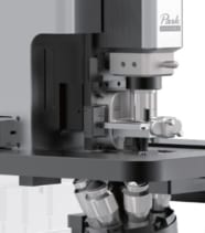
An affordable and versatile platform for analytical chemistry and electrochemistry has just been released by Park Systems. The Park NX12 combines an inverted optical microscope (IOM) with an atomic force microscope to enable advanced research on materials such as membranes, organic devices and electronics, and biological and pathological samples.

The NX12 from Park Systems“We just purchased the Park NX12 because we wanted a research-grade platform for AFM and scanning-ion conductance microscopy (SICM) that was also easy to use,” commented Dr Yixian Wang at the California State University in Los Angeles. “The Park NX12 was the only comprehensive platform that could perform all scanning probe techniques – including pipette-based SICM – while also utilizing IOM for the nanoscale measurement flexibility we needed.”

According to Park Systems, the NX12 is ideally suited for multi-user facilities, with a modular design that lends itself to further development. It has also been designed to handle the pipette probes commonly used to study the electrochemistry of transparent materials such as nanopore membranes for fuel cells and biomembranes.

You can find out about Park Systems’ full range of microscopy solutions at Booth 406.

Narrow-wavelenth laser diodes extend Raman to more wavelengths

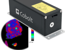
Cobolt AB, a laser manufacturer that is part of HÜBNER Photonics, has added two new laser diodes operating at 633 nm and 785 nm to its range of devices for high-resolution Raman spectroscopy. Both devices are frequency-stabilized, narrow-linewidth laser diodes with a linewidth of less than 20 pm, and both include an integrated optical isolator.

Cobolt laser diodes for Raman spectroscopyThe Cobolt 08-NLD 633 nm offers an output power of up to 30 mW, while the single-transverse mode 08-NLD 785 nm delivers up to 120 mW. All Cobolt lasers are manufactured using proprietary HTCure technology, which yields a compact hermetically sealed package for exceptional reliability in changing environmental conditions.

With a demonstrated lifetime in excess of 60,000 hours, Cobolt says that its lasers deliver excellent performance in both laboratory and industrial environments, and are offered with market-leading warranty terms.

Representatives from Cobolt will be at Booth 546 to provide more details about its full line of laser diodes and diode-pumped solid-state lasers.

Best predictions of winter gas demand are written on the wind

UK gas usage varies hugely from one winter to the next, but the industry typically predicts demand based on historical data. Now, researchers from the UK have shown that seasonal forecasts of atmospheric circulation made at the start of November are a much more skilful method of managing supplies over winter.

When the UK experienced unusually cold conditions in December 2010 and March 2018, extreme gas demand prompted operators to warn of possible shortages, and caused prices to surge. An ability to anticipate such periods weeks in advance could make gas supplies more resilient and dampen price spikes. And the same forecasting technique could potentially be applied to any other sector in which temperature and atmospheric circulation influence supply and demand, for example, wind power.

Because gas is the main source of heating for homes and businesses in the UK, it’s natural that demand rises as the temperature falls. Predict the temperature, you might think, and you should predict demand.

Unfortunately, it’s not that simple. “Successful prediction of the gas demand is a product of two components,” Adam Scaife of the UK Met Office explains: “You need a tight relationship with the weather, but also good prediction skill.”

Although winter temperatures do have this tight relationship with gas demand, over the British Isles they are curiously hard to forecast accurately. “The forecast model has a weak signal-to-noise ratio, so the predictable signal is a small component of the total variability,” says Scaife.

To find a more predictable proxy for temperature, Scaife and colleagues from the Met Office, University of Exeter, Imperial College London and University of Reading looked at the mean gas demand each winter between 1996 and 2018, and counted the number of days each year that demand was exceptional.

“The industry is extremely interested in those days, because those are the times when the demand can be so high that we start to approach the limit of our reserves for supplying the UK,” says Scaife.

The best candidates for replacing direct temperature prediction relate to large-scale pressure patterns. “The temperatures in the UK from one year to the next are pretty much entirely governed by the atmospheric circulation,” says Scaife. “It’s all about which way the wind blows.”

To make use of this, the researchers produced retrospective forecasts of large-scale atmospheric patterns for each winter covered by the gas-demand records.

A direct forecast of mean winter temperature over the UK was, as expected, an unreliable predictor of both seasonal gas demand and the number of high-demand days. Air pressure patterns over Europe and the North Atlantic, however, had much more predictive power.

A negative phase of the North Atlantic Oscillation – when the difference between the low air pressure over Iceland and high pressure over the Azores is less than usual – corresponded well with both high mean demand and the number of exceptional days. So too did the presence of a pressure gradient across the UK, with high pressure in the north and low in the south.

In previous work, the team identified four regional pressure configurations that were associated with high-demand days. The appearance of similar conditions in the current study’s forecasts was also a good predictor of both mean and exceptional gas demand.

Scaife and colleagues reported their findings in Environmental Research Letters (ERL).

Academic paediatric facilities deliver lower dose during CT exams

Monitoring the X-ray dose delivered to patients during diagnostic radiology procedures is an important precursor step in improving patient care. Keith Strauss and colleagues from Cincinnati Children’s Hospital Medical Center compared the dose delivered to children in CT examinations and found statistically significant variation in the mean dose delivered across different types of institutions.

Strauss and colleagues pooled data from 239,622 paediatric CT examinations in the Dose Index Registry from 519 medical imaging centres. They statistically tested the hypothesis that academic paediatric CT providers use diagnostic imaging protocols specifically designed for children that deliver lower radiation doses. The researchers concluded that academic paediatric centres delivered lower radiation dose across all brain examinations, and the majority of chest and pelvis examinations, compared with alternative medical imaging centres (Radiology 10.1148/radiol.2019181753).

The researchers compared patient size-adjusted dose indices across four categories of diagnostic CT providers: academic paediatric, academic adult, non-academic paediatric and non-academic adult. Imaging centres with a medical school affiliation were designated as academic; those listed by the Children’s Hospital Association as paediatric were classified as paediatric facilities.

The team chose to compare three recognised dose indices: the volume CT dose index, the size-specific dose estimate and the dose–length product. To adjust for patient size, the researchers used the patient effective diameter derived from localizer scans, which are used to check patient positioning prior to CT examination. They distributed the data into six patient size categories for chest and pelvic examinations, and five size groups for brain examinations.

Strauss and colleagues used the mean dose index from academic paediatric facilities as a benchmark and compared this value with the mean dose indices from the three remaining categories, using the unequal variance two sample t-test. Since multiple comparisons were made, the researchers also adjusted the confidence level using the Bonferroni correction.

The results showed that across all six patient size groups, and for all three dose metrics, academic paediatric facilities delivered lower mean dose than adult academic, adult non-academic and paediatric non-academic facilities, in 78% of paediatric chest exam comparisons and 89% of comparisons between pelvic exams. For paediatric brain imaging studies, the academic paediatric facilities delivered lower mean dose in all comparisons.

The researchers also compared the variance in the three radiation dose metrics across the different providers. Again, they found that the academic paediatric facilities delivered a less variable dose in the majority of comparisons.

This study highlights the role that effective dose monitoring may have on patient health and outcomes in diagnostic radiology. “Dose management is important for all patients, both paediatric and adult patients. This begins with patient dose monitoring. However, the monitoring step by itself does nothing to improve patient care. Additional steps must be taken to carefully manage the CT radiation of all patients to have a positive impact on patient care,” stresses Strauss.

Twistronics lights up with moiré exciton experiments

For the first announcement of “magic-angle” bilayer graphene’s newly discovered twist-tunable electronic properties last year, APS convened a special session in the atrium of the conference venue to accommodate the throngs of attendees eager to hear the details. Editors at Nature may have also considered convening a special section of their journal this week to accommodate the flash flood of announcements reporting evidence of a new kind of quantum optical behaviour in similar twist-tunable stacks of other types of 2D materials.

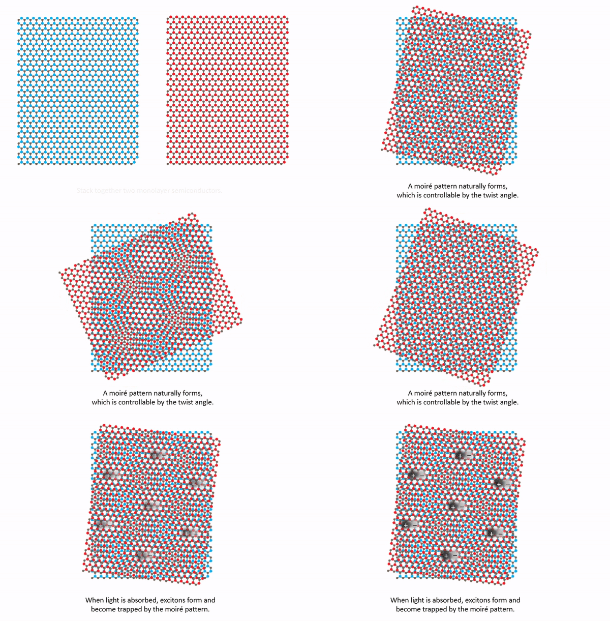
“We were actually surprised that we didn’t see the effects sooner,” says Xiaodong Xu, principle investigator at the Nanoscale Optoelectronics Laboratory at the University of Washington in the US, and a corresponding author on one of this week’s papers. No fewer than three papers reported experimental results indicating the presence of interlayer excitons trapped in the periodically dappled moiré potential field that results when two atomically thick layers of transition metal dichalcogenide (TMDs) are misaligned. Yet while Xu suggests the discoveries were in some ways due, he highlights how specific the conditions for observing interlayer trapped moiré excitons are, which may explain why they have only just been observed.

“It turns out the moiré effects can be obscured somewhat by an imperfect moiré pattern, which will lead to light emission similar to defects, and excess laser excitation power, which will provide a broad background,” Xu tells Physics World. “In fact, we have seen effects of moiré excitons several years back, but we just did not know what we were looking at and what the evidence for moiré excitons should be.  Once we started to excite the system with lower laser power and perform magneto-optical spectroscopy of samples with different twist angles, we began to realize that moiré-trapped excitons have been there all the time!”

The results highlight the “feasibility of engineering artificial excitonic crystals using van der Waals heterostructures for nanophotonics and quantum information applications” as  Fengcheng Wu at Argonne National Laboratory, Xiaoqin Li at the University of Texas at Austin and their colleagues propose in their report. In addition the work has fundamental significance, providing “an attractive platform from which to explore and control excited states of matter, such as topological excitons and a correlated exciton Hubbard model, in transition metal dichalcogenides,” according to the report by Feng Wang at the University of California, Berkeley, and co-authors.

Excitons meet 2D materials

An exciton is the quantum particle that arises as an electron couples to the quantum “hole” that is left behind when an electron is excited out of its band. They have been studied in many systems including 2D materials and TMDs. In fact the past decade has seen a surge in general in studies of TMDs – chemicals with the formula MX2 where M is a transition metal, for example molybdenum or tungsten, and X is a chalcogen such as sulphur, selenium or tellurium – particularly in the form of atomically thin 2D materials where a single layer of the metal atoms is sandwiched between two layers of the chalcogen.

Xu’s group, is one of several that have studied the optical response of monolayer TMDs for many years. He describes how a monolayer TMD behaves as a quantum well. However in addition to spin, charge carriers in TMDs have an additional “valley” degree of freedom leading to quantum wells with coupled spin-valley physics. As a result, as far back as 2013, Xu’s group started pushing the idea of stacking two monolayers on top of each other, to mimic the double quantum well structures in other materials such as III-V semiconductors like GaAs/AlGaAs. In addition, they expected the atomically thin nature of these structures would make them very tunable.

“In our previous work, we realized that the system is a very exciting platform for manipulating excitons with long life time and spin-valley degrees of freedom,” say Xu. “In developing the understanding of our experimental results, our theory collaborator Wang Yao and his postdoc Hongyi Yu at University of Hongkong realized that there exists very interesting moiré exciton physics in the twisted heterobilayer system. Since then, we have been working on the experimental realization of these moiré effects.”

moire excitons

Different ways to peel an orange

Although all three papers report moiré excitons in 2D TMDs, there are some important distinctions in what each one demonstrates. Wu, Li and colleagues studied the response of MoSe2/WSe2 heterobilayers twisted at an angle of 1° and encapsulated in hexagonal boron nitride. Their photoluminescence studies with circularly polarized light revealed peaks in the spectra indicative of excitons at four distinct energies. Since the exciton “Bohr radius” – an analogue of an atomic radius – is much smaller than the period of the moiré pattern, they attribute the four quantized energy levels to lateral confinement imposed by the moiré potential. As further support for this model, when the twist angle is increased to 2° and the moiré pattern changes, the spacing of their exciton peaks also change and increase, although at significantly larger angles they disappear altogether. Their model also suggests an explanation for the co- and cross-circular emission from their structures.

The heterostructures in the work reported by Wang and colleagues – some of whom are also collaborators with Wu, Li and colleagues – are WSe2/WS2 encapsulated in hexagonal boron nitride. These experiments include few layer graphene contacts to observe the effects of tuning the carrier doping with an applied electric field. They observe emission peaks at three slightly higher energies that weaken and also eventually disappear as the angle between the layers is increased beyond 3°. They note that exciting the sample at any of these three emission peak energies leads to strong enhancement of the interlayer exciton emission at 1.409 eV, which they suggest indicates that the three peaks arise from the strongly coupled WSe2/WS2 heterostructure rather than from several separated domains. In addition, they observe strong blue shifts in the exciton energies as doping is increased, which affects all the peaks similarly. This effect is not observed in monolayers of the materials and cannot be explained by established electron–exciton interactions in monolayers.

Applying a magnetic field reveals yet more nuances in the behaviour of the moiré excitons as Xu and colleagues report in their study of MoSe2/WSe2 superlattices. They find equal and opposing shifts for cross and co-circularly polarized light depending on the magnetic field. They demonstrated that, these slopes, representing the g factors (a dimensionless magnetic moment), are determined by valley index pairing. They also show that the twist in the lattice can compensate for momentum mismatches in the excitons so that they radiatively recombine (known as Umklapp recombination). “We show that we can use g-factors  as a fingerprint to identify moiré excitons,” Xu adds. “This approach should be applicable to understand other optical responses.”

Drawing on diverse expertise

So what brought all three reports at once? Xu suggests that advances in theory, greater availability of high-quality heterobilayer samples, and the mounting interest in moiré effects have all played a role. He highlights some of the factors that have made a difference for the Xu Lab in particular, such as the access to clean 3D bulk crystals provided by their long-term collaborators Jiaqiang Yan and David Mandrus at Oakridge National Laboratory, expertise acquired in the fabrication of structures with fine twist control as well as light emission polarization and g-factors measurements, and crucially the theoretical support from Yao to understand the measurements.

“We believe that the basic results are quite experimentally achievable in many other groups; it’s just a matter of making clean-enough samples with different twist angles and using the right experimental conditions (low excitation power, low temperature, magnetic field control, etc),” says Xu. He adds that the diverse expertise within this sector of the research community as highlighted in the differences in the reports this week, can help towards a deeper understanding of moiré excitons for both fundamental physics and potential applications. “It will be important for future progress in this new field to have productive cross-talk or collaboration between our groups and the community as a whole.”

Full details are reported in Nature at DOI: 10.1038/s41586-019-0975-z; DOI: 10.1038/s41586-019-0976-y; and DOI: 10.1038/s41586-019-0957-1

Physics World 30th anniversary podcast series – high-temperature superconductivity

Physics World has recently turned 30 and we are celebrating with a five-part podcast series exploring key areas of physics. This fourth episode in the series explores how high-temperature superconductivity research has evolved over the past three decades since the phenomenon was first observed.

In the late 1980s there was a lot of hype surrounding these materials because of the many exciting applications that would follow. Among the promised spin-offs were lossless transmission lines, lossless magnetism and levitating trains. All of these applications have been demonstrated to some extent but it is also fair to say that high-temperature superconductors are not as ubiquitous as some had hoped.

In this podcast, Andrew Glester picks up the story to find out more about the history of high-temperature superconductivity and its prospects for the future. He catches up with the physicists Elizabeth Blackburn from Lund University in Sweden and Stephen Hayden from the University of Bristol, UK.

If you enjoy the podcast, then take a listen to the first three podcasts in the 30th anniversary series. Glester began in October by looking at the past and future of particle physics before tackling gravitational waves in November and then nuclear fusion in January. Don’t forget you can also subscribe to Physics World Stories via Apple podcasts or your chosen podcast host.

Copyright © 2025 by IOP Publishing Ltd and individual contributors