This episode of the Physics World Weekly podcast explores how quantum computing and artificial intelligence can be combined to help physicists search for rare interactions in data from an upgraded Large Hadron Collider.
My guest is Javier Toledo-Marín, and we spoke at the Perimeter Institute in Waterloo, Canada. As well as having an appointment at Perimeter, Toledo-Marín is also associated with the TRIUMF accelerator centre in Vancouver.
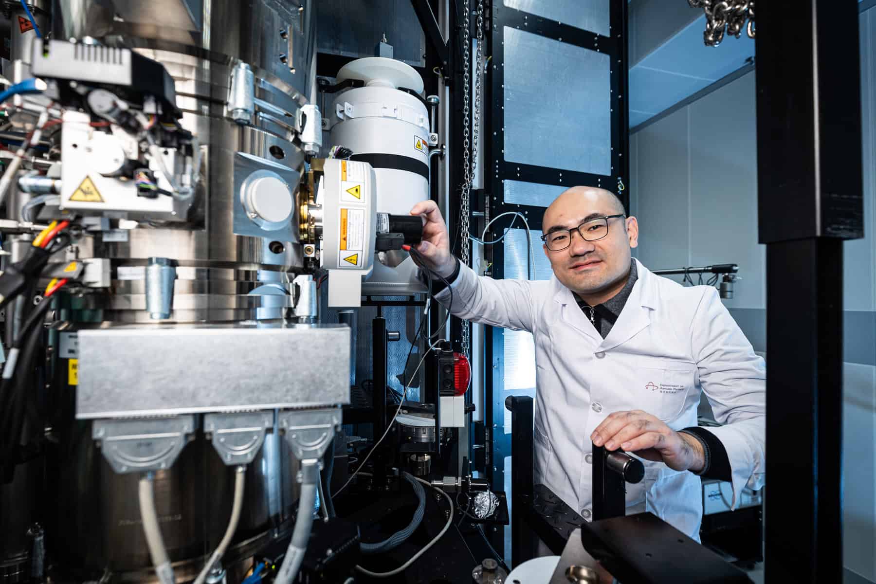
Professor Zhao Jiong, who leads a Master’s programme in microelectronics technology and material, has been recognized for his pioneering research in 2d ferroelectronics (Courtesy: PolyU)
The microelectronics sector is known for its relentless drive for innovation, continually delivering performance and efficiency gains within ever more compact form factors. Anyone aspiring to build a career in this fast-moving field needs not just a thorough grounding in current tools and techniques, but also an understanding of the next-generation materials and structures that will propel future progress.
That’s the premise behind a Master’s programme in microelectronics technology and materials at the Hong Kong Polytechnic University (PolyU). Delivered by the Department for Applied Physics, globally recognized for its pioneering research in technologies such as two-dimensional materials, nanoelectronics and artificial intelligence, the aim is to provide students with both the fundamental knowledge and practical skills they need to kickstart their professional future – whether they choose to pursue further research or to find a job in industry.
“The programme provides students with all the key skills they need to work in microelectronics, such as circuit design, materials processing and failure analysis,” says programme leader Professor Zhao Jiong, who research focuses on 2D ferroelectrics. “But they also have direct access to more than 20 faculty members who are actively investigating novel materials and structures that go beyond silicon-based technologies.”
The course in also unusual in providing a combined focus on electronics engineering and materials science, providing students with a thorough understanding of the underlying semiconductors and device structures as well as their use in mass-produced integrated circuits. That fundamental knowledge is reinforced through regular experimental work, providing the students with hands-on experience of fabricating and testing electronic devices. “Our cleanroom laboratory is equipped with many different instruments for microfabrication, including thin-film deposition, etching and photolithography, as well as advanced characterization tools for understanding their operating mechanisms and evaluating their performance,” adds Zhao.
In a module focusing on thin-film materials, for example, students gain valuable experience from practical sessions that enable them to operate the equipment for different growth techniques, such as sputtering, molecular beam epitaxy, and both physical and chemical vapour deposition. In another module on materials analysis and characterization, the students are tasked with analysing the layered structure of a standard computer chip by making cross-sections that can be studied with a scanning electron microscope.
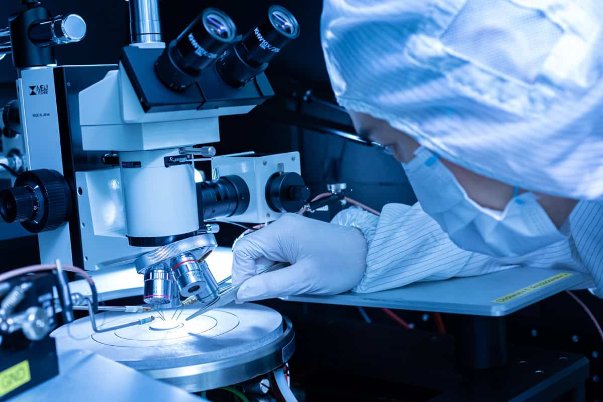
During the programme students have access to a cleanroom laboratory that gives them hand-on experience of using advanced tools for fabricating and characterizing electronic materials and structures (Courtesy: PolyU)
That practical experience extends to circuit design, with students learning how to use state-of-the-art software tools for configuring, simulating and analysing complex electronic layouts. “Through this experimental work students gain the technical skills they need to design and fabricate integrated circuits, and to optimize their performance and reliability through techniques like failure analysis,” says Professor Dai Jiyan, PolyU Associate Dean of Students, who also teaches the module on thin-film materials. “This hands-on experience helps to prepare them for working in a manufacturing facility or for continuing their studies at the PhD level.”
Also integrated into the teaching programme is the use of artificial intelligence to assist key tasks, such as defect analysis, materials selection and image processing. Indeed, PolyU has established a joint laboratory with Huawei to investigate possible applications of AI tools in electronic design, providing the students with early exposure to emerging computational methods that are likely to shape the future of the microelectronics industry. “One of our key characteristics is that we embed AI into our teaching and laboratory work,” says Dai. “Two of the modules are directly related to AI, while the joint lab with Huawei helps students to experiment with using AI in circuit design.”
Now in its third year, the Master’s programme was designed in collaboration with Hong Kong’s Applied Science and Technology Research Institute (ASTRI), established in 2000 to enhance the competitiveness of the region through the use of advanced technologies. Researchers at PolyU already pursue joint projects with ASTRI in areas like chip design, microfabrication and failure analysis. As part of the programme, these collaborators are often invited to give guest lectures or to guide the laboratory work. “Sometimes they even provide some specialized instruments for the students to use in their experiments,” says Zhao. “We really benefit from this collaboration.”
Once primed with the knowledge and experience from the taught modules, the students have the opportunity to work alongside one of the faculty members on a short research project. They can choose whether to focus on a topic that is relevant to present-day manufacturing, such as materials processing or advanced packaging technologies, or to explore the potential of emerging materials and devices across applications ranging from solar cells and microfluidics to next-generation memories and neuromorphic computing.
“It’s very interesting for the students to get involved in these projects,” says Zhao. “They learn more about the research process, which can make them more confident to take their studies to the next level. All of our faculty members are engaged in important work, and we can guide the students towards a future research field if that’s what they are interested in.”
There are also plenty of progression opportunities for those who are more interested in pursuing a career in industry. As well as providing support and advice through its joint lab in AI, Huawei arranges visits to its manufacturing facilities and offers some internships to interested students. PolyU also organizes visits to Hong Kong’s Science Park, home to multinational companies such as Infineon as well as a large number of start-up companies in the microelectronics sector. Some of these might support a student’s research project, or offer an internship in areas such as circuit design or microfabrication.
The international outlook offered by PolyU has made the Master’s programme particularly appealing to students from mainland China, but Zhao and Dai believe that the forward-looking ethos of the course should make it an appealing option for graduates across Asia and beyond. “Through the programme, the students gain knowledge about all aspects of the microelectronics industry, and how it is likely to evolve in the future,” says Dai. “The knowledge and technical skills gained by the students offer them a competitive edge for building their future career, whether they want to find a job in industry or to continue their research studies.”
Pancreatic ductal adenocarcinoma (PDAC), the most common type of pancreatic cancer, is an aggressive tumour with a poor prognosis. Surgery remains the only potential cure, but is feasible in just 10–15% of cases. A team headed up at Sichuan University in China has now developed a selective laser ablation technique designed to target PDAC while leaving healthy pancreatic tissue intact.
Thermal ablation techniques, such as radiofrequency, microwave or laser ablation, could provide a treatment option for patients with locally advanced PDAC, but existing methods risk damaging surrounding blood vessels and healthy pancreatic tissues. The new approach, described in Optica, uses the molecular fingerprint of pancreatic tumours to enable selective ablation.
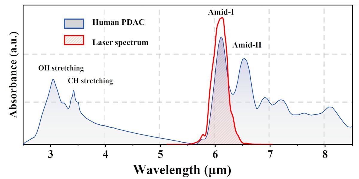
The technique exploits the fact that PDAC tissue contains a large amount of collagen compared with healthy pancreatic tissue. Amide-I collagen fibres exhibit a strong absorption peak at 6.1 µm, thus the researchers surmised that tuning the treatment laser to this resonant wavelength could enable efficient tumour ablation with minimal collateral thermal damage. As such, they designed a femtosecond pulsed laser that can deliver 6.1 µm pulses with a power of more than 1 W.
Resonant wavelength Fourier-transform infrared spectra of PDAC (blue) and the laser (red). (Courtesy: Houkun Liang, Sichuan University)
“We developed a mid-infrared femtosecond laser system for the selective tissue ablation experiment,” says team leader Houkun Liang. “The system is tunable in the wavelength range of 5 to 11 µm, aligning with various molecular fingerprint absorption peaks such as amide proteins, cholesteryl ester, hydroxyapatite and so on.”
Liang and colleagues first examined the ablation efficiency of three different laser wavelengths on two types of pancreatic cancer cells. Compared with non-resonant wavelengths of 1 and 3 µm, the collagen-resonant 6.1 µm laser was far more effective in killing pancreatic cancer cells, reducing cell viability to ranges of 0.27–0.32 and 0.37–0.38, at 0 and 24 h, respectively.
The team observed similar results in experiments on ectopic PDAC tumours cultured on the backs of mice. Irradiation at 6.1 µm led to five to 10 times deeper tumour ablation than seen for the non-resonant wavelengths (despite using a laser power of 5 W for 1 µm ablation and just 500 mW for 6.1 and 3 µm), indicating that 6.1 µm is the optimal wavelength for PDAC ablation surgery.
To validate the feasibility and safety of 6.1 µm laser irradiation, the team used the technique to treat PDAC tumours on live mice. Nine days after ablation, the tumour growth rate in treated mice was significantly suppressed, with an average tumour volume of 35.3 mm3. In contrast, tumour volume in a control group of untreated mice reached an average of 292.7 mm3, roughly eight times the size of the ablated tumours. No adverse symptoms were observed following the treatment.
Clinical potential
The researchers also used 6.1 µm laser irradiation to ablate pancreatic tissue samples (including normal tissue and PDAC) from 13 patients undergoing surgical resection. They used a laser power of 1 W and four scanning speeds (0.5, 1, 2 and 3 mm/s) with 10 ablation passes, examining 20 to 40 samples for each parameter.
At the slower scanning speeds, excessive energy accumulation resulted in comparable ablation depths. At speeds of 2 or 3 mm/s, however, the average ablation depths in PDAC samples were 2.30 and 2.57 times greater than in normal pancreatic tissue, respectively, demonstrating the sought-after selective ablation. At 3 mm/s, for example, the ablation depth in tumour was 1659.09±405.97 µm, compared with 702.5±298.32 µm in normal pancreas.
The findings show that by carefully controlling the laser power, scanning speed and number of passes, near-complete ablation of PDACs can be achieved, with minimal damage to surrounding healthy tissues.
To further investigate the clinical potential of this technique, the researchers developed an anti-resonant hollow-core fibre (AR-HCF) that can deliver high-power 6.1 µm laser pulses deep inside the human body. The fibre has a core diameter of approximately 113 µm and low bending losses at radii under 10 cm. The researchers used the AR-HCF to perform 6.1 µm laser ablation of PDAC and normal pancreas samples. The ablation depth in PDAC was greater than in normal pancreas, confirming the selective ablation properties.
“We are working together with a company to make a medical-grade fibre system to deliver the mid-infrared femtosecond laser. It consists of AR-HCF to transmit mid-infrared femtosecond pulses, a puncture needle and a fibre lens to focus the light and prevent liquid tissue getting into the fibre,” explains Liang. “We are also making efforts to integrate an imaging unit into the fibre delivery system, which will enable real-time monitoring and precise surgical guidance.”
Next, the researchers aim to further optimize the laser parameters and delivery systems to improve ablation efficiency and stability. They also plan to explore the applicability of selective laser ablation to other tumour types with distinct molecular signatures, and to conduct larger-scale animal studies to verify long-term safety and therapeutic outcomes.
“Before this technology can be used for clinical applications, highly comprehensive biological safety assessments are necessary,” Liang emphasizes. “Designing well-structured clinical trials to assess efficacy and risks, as well as navigating regulatory and ethical approvals, will be critical steps toward translation. There is a long way to go.”
Low-energy electrons escape from some materials via distinct “doorway” states, according to a study done by physicists at Austria’s Vienna Institute of Technology. The team studied graphene-based materials and found that the nature of the doorway states depended on the number of graphene layers in the sample.
Low-energy electron (LEE) emission from solids is used across a range of materials analysis and processing applications including scanning electron microscopy and electron-beam induced deposition. However, the precise physics of the emission process is not well understood.
Electrons are ejected from a material when a beam of electrons is fired at its surface. Some of these incident electrons will impart energy to electrons residing in the material, causing some resident electrons to be emitted from the surface. In the simplest model, the minimum energy needed for this LEE emission is the electron binding energy of the material.
Frog in a box
In this new study, however, researchers have shown that exceeding the binding energy is not enough for LEE emission from graphene-based materials. Not only does the electron need this minimum energy, it must also be in a specific doorway state or it is unlikely to escape. The team compare this phenomenon to the predicament of a frog in a cardboard box with a window. Not only must the frog hop a certain height to escape the box, it must also begin its hop from a position that will result in it travelling through the hole (see figure).
For most materials, the energy spectrum of LEE electrons is featureless. However, it was known that graphite’s spectrum has an “X state” at about 3.3 eV, where emission is enhanced. This state could be related to doorway states.
To search for doorway states, the Vienna team studied LEE emission from graphite as well as from single-layer and bi-layer graphene. Graphene is a sheet of carbon just one atom thick. Sheets can stick together via the relatively weak Van der Waals force to create multilayer graphene – and ultimately graphite, which comprises a large number of layers.
Because electrons are mostly confined within the graphene layers, the electronic states of single-layer, bi-layer and multi-layer graphene are broadly similar. As a result, it was expected that these materials would have similar LEE emission spectra . However, the Vienna team found a surprising difference.
Emission and reflection
The team made their discovery by firing a beam of relatively low energy electrons (173 eV) incident at 60° to the surface of single-layer and bi-layer graphene as well as graphite. The scattered electrons are then detected at the same angle of reflection. Meanwhile, a second detector is pointed normal to the surface to capture any emitted electrons. In quantum mechanics electrons are indistinguishable, so the modifiers scattered and emitted are illustrative, rather than precise.
The team looked for coincident signals in both detectors and plotted their results as a function of energy in 2D “heat maps”. These plots revealed that bi-layer graphene and graphite each had doorway states – but at different energies. However, single-layer graphene did not appear to have any doorway states. By combining experiments with calculations, the team showed that doorway states emerge above a certain number of layers. As a result the researchers showed that graphite’s X state can be attributed in part to a doorway state that appears at about five layers of graphene.
“For the first time, we’ve shown that the shape of the electron spectrum depends not only on the material itself, but crucially on whether and where such resonant doorway states exist,” explains Anna Niggas at the Vienna Institute of Technology.
As well as providing important insights in how the electronic properties of graphene morph into the properties of graphite, the team says that their research could also shed light on the properties of other layered materials.
NASA’s Jet Propulsion Laboratory (JPL) is to lay off some 550 employees as part of a restructuring that began in July. The action affects about 11% of JPL’s employees and represents the lab’s third downsizing in the past 20 months. When the layoffs are complete by the end of the year, the lab will have roughly 4500 employees, down from about 6500 at the start of 2024. A further 4000 employees have already left NASA during the past six months via sacking, retirement or voluntary buyouts.
Managed by the California Institute of Technology in Pasadena, JPL oversees scientific missions such as the Psyche asteroid probe, the Europa Clipper and the Perseverance rover on Mars. The lab also operates the Deep Space Network that keeps Earth in communication with unmanned space missions. JPL bosses already laid off about 530 staff – and 140 contractors – in February last year followed by another 325 people in November 2024.
JPL director Dave Gallagher insists, however, that the new layoffs are not related to the current US government shutdown that began on 1 October. “[They are] essential to securing JPL’s future by creating a leaner infrastructure, focusing on our core technical capabilities, maintaining fiscal discipline, and positioning us to compete in the evolving space ecosystem,” he says in a message to employees.
Judy Chu, Democratic Congresswoman for the constituency that includes JPL, is less optimistic. “Every layoff devastates the highly skilled and uniquely talented workforce that has made these accomplishments possible,” she says. “Together with last year’s layoffs, this will result in an untold loss of scientific knowledge and expertise that threatens the very future of American leadership in space exploration and scientific discovery.”
John Logsdon, professor emeritus at George Washington University and founder of the university’s Space Policy Institute, says that the cuts are a direct result of the Trump administration’s approach to science and technology. “The administration gives low priority to robotic science and exploration, and has made draconic cuts to the science budget; that budget supports JPL’s work,” he told Physics World. “With these cuts, there is not enough money to support a JPL workforce sized for more ambitious activities. Ergo, staff cuts.”
I hugely enjoyed physics when I was a youngster. I had the opportunity both at home and school to create my own projects, which saw me make electronic circuits, crazy flying models like delta-wings and autogiros, and even a gas chromatograph with a home-made chart recorder. Eventually, this experience made me good enough to repair TV sets, and work in an R&D lab in the holidays devising new electronic flow controls.
That enjoyment continued beyond school. I ended up doing a physics degree at the University of Oxford before working on the discovery of the gluon at the DESY lab in Hamburg for my PhD. Since then I have used physics in industry – first with British Oxygen/Linde and later with Air Products & Chemicals – to solve all sorts of different problems, build innovative devices and file patents.
While some students have a similarly positive school experience and subsequent career path, not enough do. Quite simply, physics at school is the key to so many important, useful developments, both within and beyond physics. But we have a physics education problem, or to put it another way – a “future of physics” problem.
There are just not enough school students enjoying and learning physics. On top of that there are not enough teachers enjoying physics and not enough students doing practical physics. The education problem is bad for physics and for many other subjects that draw on physics. Alas, it’s not a new problem but one that has been developing for years.
Problem solving
Many good points about the future of physics learning were made by the Institute of Physics in its 2024 report Fundamentals of 11 to 19 Physics. The report called for more physics lessons to have a practical element and encouraged more 16-year-old students in England, Wales and Northern Ireland to take AS-level physics at 17 so that they carry their GCSE learning at least one step further.
Doing so would furnish students who are aiming to study another science or a technical subject with the necessary skills and give them the option to take physics A-level. Another recommendation is to link physics more closely to T-levels – two-year vocational courses in England for 16–19 year olds that are equivalent to A-levels – so that students following that path get a background in key aspects of physics, for example in engineering, construction, design and health.
But do all these suggestions solve the problem? I don’t think they are enough and we need to go further. The key change to fix the problem, I believe, is to have student groups invent, build and test their own projects. Ideally this should happen before GCSE level so that students have the enthusiasm and background knowledge to carry them happily forward into A-level physics. They will benefit from “pull learning” – pulling in knowledge and active learning that they will remember for life. And they will acquire wider life skills too.
Developing skillsets
During my time in industry, I did outreach work with schools every few weeks and gave talks with demonstrations at the Royal Institution and the Franklin Institute. For many years I also ran a Saturday Science club in Guildford, Surrey, for pupils aged 8–15.
Based on this, I wrote four Saturday Science books about the manyplayful and original demonstrations and projects that came out of it. Then at the University of Surrey, as a visiting professor, I had small teams of final-year students who devised extraordinary engineering – designing superguns for space launches, 3D printers for full-size buildings and volcanic power plants inter alia. A bonus was that other staff working with the students got more adventurous too.
But that was working with students already committed to a scientific path. So lately I’ve been working with teachers to get students to devise and build their own innovative projects. We’ve had 14–15-year-old state-school students in groups of three or four, brainstorming projects, sketching possible designs, and gathering background information. We help them and get A-level students to help too (who gain teaching experience in the process). Students not only learn physics better but also pick up important life skills like brainstorming, team-working, practical work, analysis and presentations.
We’ve seen lots of ingenuity and some great projects such as an ultrasonic scanner to sense wetness of cloth; a system to teach guitar by lighting up LEDs along the guitar neck; and measuring breathing using light passing through a band of Lycra around the patient below the ribs. We’ve seen the value of failure, both mistakes and genuine technical problems.
Best of all, we’ve also noticed what might be dubbed the “combination bonus” – students having to think about how they combine their knowledge of one area of physics with another. A project involving a sensor, for example, will often involve electronics as well the physics of the sensor and so student knowledge of both areas is enhanced.
Some teachers may question how you mark such projects. The answer is don’t mark them! Project work and especially group work is difficult to mark fairly and accurately, and the enthusiasm and increased learning by students working on innovative projects will feed through into standard school exam results.
Not trying to grade such projects will mean more students go on to study physics further, potentially to do a physics-related extended project qualification – equivalent to half an A-level where students research a topic to university level – and do it well. Long term, more students will take physics with them into the world of work, from physics to engineering or medicine, from research to design or teaching.
Such projects are often fun for students and teachers. Teachers are often intrigued and amazed by students’ ideas and ingenuity. So, let’s choose to do student-invented project work at school and let’s finally solve the future of physics problem.
The control of large, strongly coupled, multi-component quantum systems with complex dynamics is a challenging task.
It is, however, an essential prerequisite for the design of quantum computing platforms and for the benchmarking of quantum simulators.
A key concept here is that of quantum ergodicity. This is because quantum ergodic dynamics can be harnessed to generate highly entangled quantum states.
In classical statistical mechanics, an ergodic system evolving over time will explore all possible microstates states uniformly. Mathematically, this means that a sufficiently large collection of random samples from an ergodic process can represent the average statistical properties of the entire process.
Quantum ergodicity is simply the extension of this concept to the quantum realm.
Closely related to this is the idea of chaos. A chaotic system is one in which is very sensitive to its initial conditions. Small changes can be amplified over time, causing large changes in the future.
The ideas of chaos and ergodicity are intrinsically linked as chaotic dynamics often enable ergodicity.
Until now, it has been very challenging to predict which experimentally preparable initial states will trigger quantum chaos and ergodic dynamics over a reasonable time scale.
In a new paper published in Reports on Progress in Physics, a team of researchers have proposed an ingenious solution to this problem using the Bose–Hubbard Hamiltonian.
They took as an example ultracold atoms in an optical lattice (a typical choice for experiments in this field) to benchmark their method.
The results show that there are certain tangible threshold values which must be crossed in order to ensure the onset of quantum chaos.
These results will be invaluable for experimentalists working across a wide range of quantum sciences.
Precision measurements of theoretical parameters are a core element of the scientific program of experiments at the Large Hadron Collider (LHC) as well as other particle colliders.
These are often performed using statistical techniques such as the method of maximum likelihood. However, given the size of datasets generated, reduction techniques, such as grouping data into bins, are often necessary.
These can lead to a loss of sensitivity, particularly in non-linear cases like off-shell Higgs boson production and effective field theory measurements. The non-linearity in these cases comes from quantum interference and traditional methods are unable to optimally distinguish the signal from background.
In this paper, the ATLAS collaboration pioneered the use of a neural network based technique called neural simulation-based inference (NSBI) to combat these issues.
A neural network is a machine learning model originally inspired by how the human brain works. It’s made up of layers of interconnected units called neurons, which process information and learn patterns from data. Each neuron receives input, performs a simple calculation, and passes the result to other neurons.
NSBI uses these neural networks to analyse each particle collision event individually, preserving more information and improving accuracy.
The framework developed here can handle many sources of uncertainty and includes tools to measure how confident scientists can be in their results.
The researchers benchmarked their method by using it to calculate the Higgs boson signal strength and compared it to previous methods with impressive results (see here for more details about this).
The greatly improved sensitivity gained from using this method will be invaluable in the search for physics beyond the Standard Model in future experiments at ATLAS and beyond.
When diamond defects emit light, how much of that light can be captured and used for quantum technology applications? According to researchers at the Hebrew University of Jerusalem, Israel and Humboldt Universität of Berlin, Germany, the answer is “nearly all of it”. Their technique, which relies on positioning a nanoscale diamond at an optimal location within a chip-integrated nanoantenna, could lead to improvements in quantum communication and quantum sensing.
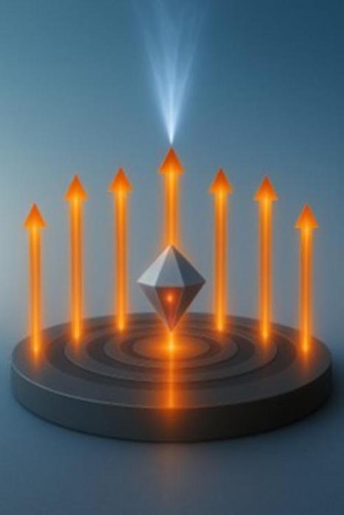
Guided light: Illustration showing photon emission from a nanodiamond and light directed by a bullseye antenna. (Courtesy: Boaz Lubotzky)
Nitrogen-vacancy (NV) centres are point defects that occur when one carbon atom in diamond’s lattice structure is replaced by a nitrogen atom next to an empty lattice site (a vacancy). Together, this nitrogen atom and its adjacent vacancy behave like a negatively charged entity with an intrinsic quantum spin.
When excited with laser light, an electron in an NV centre can be promoted into an excited state. As the electron decays back to the ground state, it emits light. The exact absorption-and-emission process is complicated by the fact that both the ground state and the excited state of the NV centre have three sublevels (spin triplet states). However, by exciting an individual NV centre repeatedly and collecting the photons it emits, it is possible to determine the spin state of the centre.
The problem, explains Boaz Lubotzky, who co-led this research effort together with his colleague Ronen Rapaport, is that NV centres radiate over a wide range of angles. Hence, without an efficient collection interface, much of the light they emit is lost.
Standard optics capture around 80% of the light
Lubotzky and colleagues say they have now solved this problem thanks to a hybrid nanostructure made from a PMMA dielectric layer above a silver grating. This grating is arranged in a precise bullseye pattern that accurately guides light in a well-defined direction thanks to constructive interference. Using a nanometre-accurate positioning technique, the researchers placed the nanodiamond containing the NV centres exactly at the optimal location for light collection: right at the centre of the bullseye.
For standard optics with a numerical aperture (NA) of about 0.5, the team found that the system captures around 80% of the light emitted from the NV centres. When NA >0.7, this value exceeds 90%, while for NA > 0.8, Lubotzky says it approaches unity.
“The device provides a chip-based, room-temperature interface that makes NV emission far more directional, so a larger fraction of photons can be captured by standard lenses or coupled into fibres and photonic chips,” he tells Physics World. “Collecting more photons translates into faster measurements, higher sensitivity and lower power, thereby turning NV centres into compact precision sensors and also into brighter, easier-to-use single-photon sources for secure quantum communication.”
The researchers say their next priority is to transition their prototype into a plug-and-play, room-temperature module – one that is fully packaged and directly coupled to fibres or photonic chips – with wafer-level deterministic placement for arrays. “In parallel, we will be leveraging the enhanced collection for NV-based magnetometry, aiming for faster, lower-power measurements with improved readout fidelity,” says Lubotzky. “This is important because it will allow us to avoid repeated averaging and enable fast, reliable operation in quantum sensors and processors.”
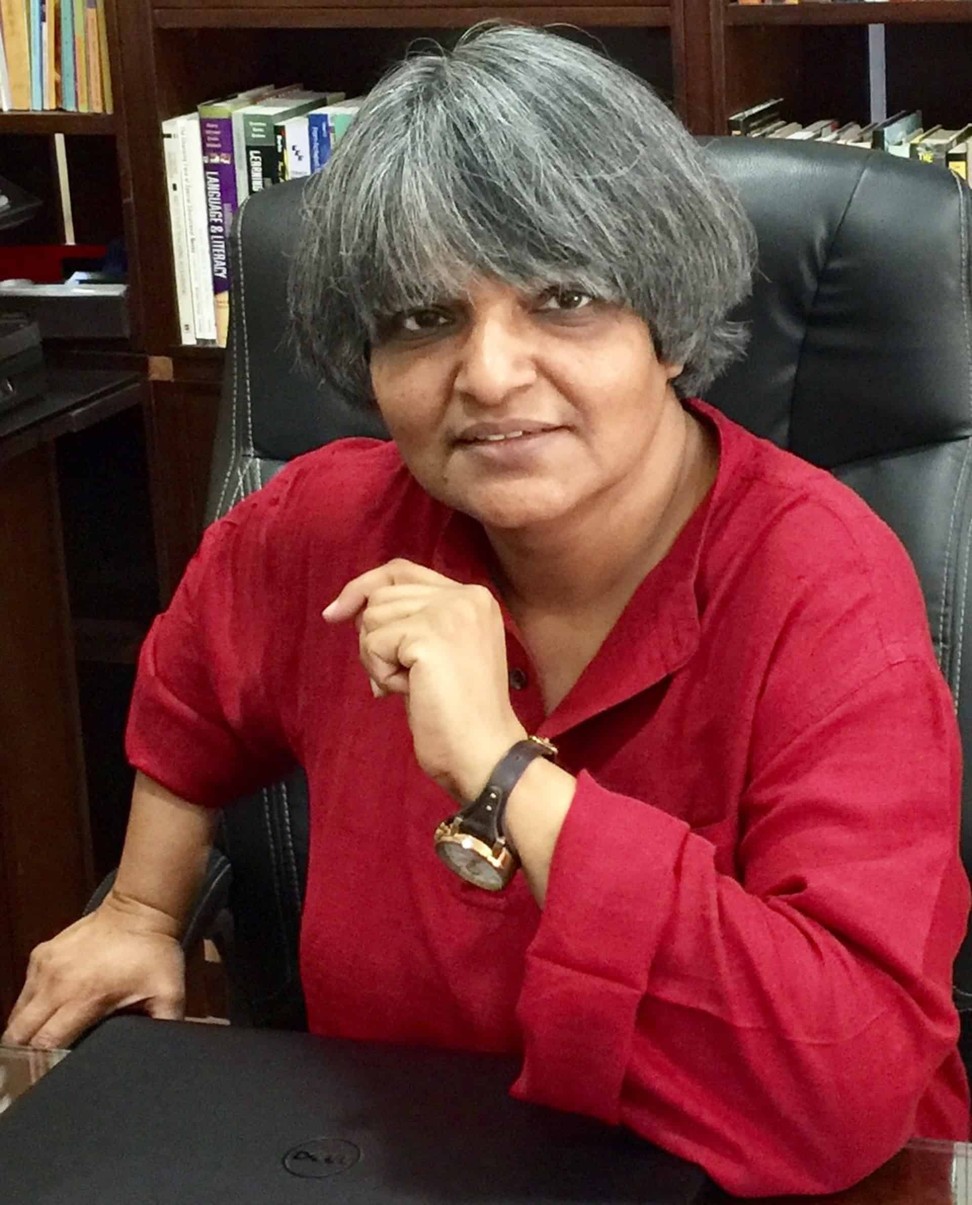
Homes and cities around the world are this week celebrating Diwali or Deepavali – the Indian “festival of lights”. For Indian physicist Rupamanjari Ghosh, who is the former vice chancellor of Shiv Nadar University Delhi-NCR, this festival sheds light on the quantum world. Known for her work on nonlinear optics and entangled photons, Ghosh finds a deep resonance between the symbolism of Diwali and the ongoing revolution in quantum science.
“Diwali comes from Deepavali, meaning a ‘row of lights’. It marks the triumph of light over dark; good over evil; and knowledge over ignorance,” Ghosh explains. “In science too, every discovery is a Diwali – a victory of knowledge over ignorance.”
With 2025 being marked by the International Year of Quantum Science and Technology, a victory of knowledge over ignorance couldn’t ring truer. “It has taken us a hundred years since the birth of quantum mechanics to arrive at this point, where quantum technologies are poised to transform our lives,” says Ghosh.
Ghosh’s career in physics took off in the mid-1980s, when she and American physicist Leonard Mandel – who is often referred to as one of the founding fathers of quantum optics – demonstrated a new quantum source of twin photons through spontaneous parametric down-conversion: a process where a high-energy photon splits into two lower-energy, correlated photons (Phys. Rev. Lett.59, 1903).
“Before that,” she recalls, “no-one was looking for quantum effects in this nonlinear optical process. The correlations between the photons defied classical explanation. It was an elegant early verification of quantum nonlocality.”
Those entangled photon pairs are now the building blocks of quantum communication and computation. “We’re living through another Diwali of light,” she says, “where theoretical understanding and experimental innovation illuminate each other.”
Entangled light
During Diwali, lamps unite households in a shimmering network of connection, and so too does entanglement of photons. “Quantum entanglement reminds us that connection transcends locality,” Ghosh says. “In the same way, the lights of Diwali connect us across borders and cultures through shared histories.”
Her own research extends that metaphor further. Ghosh’s team has worked on mapping quantum states of light onto collective atomic excitations. These “slow-light” techniques – using electromagnetically induced transparency or Raman interactions – allow photons to be stored and retrieved, forming the backbone of long-distance quantum communication (Phys. Rev. A.88 023852, EPL105 44002)
“Symbolically,” she adds, “it’s like passing the flame from one diya (lamp) to another. We’re not just spreading light – we’re preserving, encoding and transmitting it. Success comes through connection and collaboration.”
Beyond the shadows: Ghosh calls for the bright light of inclusivity in science. (Courtesy: Rupamanjari Ghosh)
The dark side of light
Ghosh is quick to note that in quantum physics, “darkness” is far from empty. “In quantum optics, even the vacuum is rich – with fluctuations that are essential to our understanding of the universe.”
Her group studies the transition from quantum to classical systems, using techniques such as error correction, shielding and coherence-preserving materials. “Decoherence – the loss of quantum behaviour through environmental interaction – is a constant threat. To build reliable quantum technologies, we must engineer around this fragility,” Ghosh explains.
There are also human-engineered shadows: some weaknesses in quantum communication devices aren’t due to the science itself – they come from mistakes or flaws in how humans built them. Hackers can exploit these “side channels” to get around security. “Security,” she warns, “is only as strong as the weakest engineering link.”
Beyond the lab, Ghosh finds poetic meaning in these challenges. “Decoherence isn’t just a technical problem – it helps us understand the arrows of time, why the universe evolves irreversibly. The dark side has its own lessons.”
Lighting every corner
For Ghosh, Diwali’s illumination is also a call for inclusivity in science. “No corner should remain dark,” she says. “Science thrives on diversity. Diverse teams ask broader questions and imagine richer answers. It’s not just morally right – it’s good for science.”
She argues that equity is not sameness but recognition of uniqueness. “Innovation doesn’t come from conformity. Gender diversity, for example, brings varied cognitive and collaborative styles – essential in a field like quantum science, where intuition is constantly stretched.”
The shadows she worries most about are not in the lab, but in academia itself. “Unconscious biases in mentorship or gatekeeping in opportunity can accumulate to limit visibility. Institutions must name and dismantle these hidden shadows through structural and cultural change.”
Her vision of inclusion extends beyond gender. “We shouldn’t think of work and life as opposing realms to ‘balance’,” she says. “It’s about creating harmony among all dimensions of life – work, family, learning, rejuvenation. That’s where true brilliance comes from.”
As the rows of diyas are lit this Diwali, Ghosh’s reflections remind us that light – whether classical or quantum – is both a physical and moral force: it connects, illuminates and endures. “Each advance in quantum science,” she concludes, “is another step in the age-old journey from darkness to light.”