Nanomaterials with advanced functional properties can enable unconventional transistor architectures and devices that exceed the sensitivity of the human skin, as Wenzhuo Wu told Physics World at innoLAE 2018 in Cambridge, UK. He described the piezotronic transistor – first introduced by Zhong Lin Wang at Georgia Institute of Technology in 2007 – and some of the research on nanowire arrays and 2D materials currently underway at his lab in Purdue University. He also highlighted the importance of work to manufacture and integrate materials into functioning devices, as well as analysis of new functional materials.
About Wenzhuo Wu
Wenzhuo Wu is assistant professor of industrial engineering at Purdue University in the US. He graduated in electronic science and technology at the University of Science and Technology of China in 2005 and received a Master’s in electrical engineering at the National University of Singapore in 2008. He completed his PhD in Zhong Lin Wang’s lab at Georgia Institute of Technology in 2013, and stayed to pursue a postdoctoral fellowship until 2015 before moving to Purdue University. He worked on the smart skin device discussed in the video during his PhD at Georgia Tech. His research interests include nanomanufacturing, self-powered nanosystems, renewable energy, human-integrated technologies and smart sensors and electronics.
The Montreal Protocol is a spectacular environmental success story. Since 2010 – 21 years after the agreement was signed by 197 parties – levels of stratospheric ozone have stabilized, and there are signs of recovery for the Antarctic ozone hole. But there is still work to be done. One ozone-depleting substance – carbon tetrachloride – has measured emissions far outweighing reported emissions. A new study reveals the likely sources.
As well as depleting ozone, carbon tetrachloride (CCl4 or CTC) is a greenhouse gas and carcinogenic in high concentrations. It plays a major role in destroying ozone, and is practically banned under the Montreal Protocol. Emissions derived from industry estimates suggest that just 3Gg of carbon tetrachloride are released globally every year. But estimates based on ground observations indicate that around 35Gg of carbon tetrachloride is added to the atmosphere every year.
Qing Liang from the NASA Goddard Space Flight Center, US, and colleagues tried to pin down the cause of this discrepancy by calculating the likely emissions from industrial sources and legacy emissions for the year 2014. They gathered data and calculated potential emissions from four different sources of carbon tetrachloride: the production and use of chlorine gas, the production of chloromethanes (used to make numerous industrial solvents for dry cleaning, paint stripping etc.), contained usages of carbon tetrachloride, and historic emissions from contaminated landfill and soil.
Chlorine is commonly used for paper bleaching and disinfection, and is usually produced in chlor-alkali plants. However, during the production process hydrocarbons can be chlorinated relatively easily, inadvertently releasing carbon tetrachloride. Liang and colleagues estimate that this, together with legacy emissions, could be responsible for up to 10Gg per year.
Chloromethanes are present in numerous industrial solvents and reagents, such as those for dry-cleaning and paint stripping. They are also a precursor in Teflon production. This process produces carbon tetrachloride that is supposed to be disposed of, usually via incineration, so its emissions of the compound should be negligible.
However, Liang and colleagues estimate that carbon tetrachloride emissions during production of the substance itself could be as high as 15Gg per year. “Because CTC evaporates easily emissions can easily occur during CTC production, unless tightly contained,” said Liang. “While deliberate production, usage, and destruction of CTC are accurately monitored and reported, unintentional CTC leakage to the atmosphere occurs.”
Finally, those carbon tetrachloride emissions from historic industrial sites and landfill. Liang and colleagues estimate that this contributes a few Gg per year. In total the new estimates suggest that these industrial and legacy sources release around 25Gg of carbon tetrachloride to the atmosphere each year; a figure considerably larger than the reported 3Gg, but still 10Gg short of the 35Gg per year estimated by satellite observations.
“If the current CTC emissions continue into the future, it will lead to an extra 5% increase in atmospheric chlorine and bromine abundance between 2050–2100 and a corresponding ~3% decrease in Antarctic total column ozone,” said Liang, whose findings are published in Environmental Research Letters (ERL). The scientists intend to try and gather more detailed data from under-reported industrial regions.
Have you ever wondered why some butterflies and fruits can shine with a metallic, iridescent blue and beetles can decorate themselves with golden shells – but there is no paint that lets you depict these dynamic colours directly? Well, it all comes down to how those organisms create the colour.
Paints and pigments simply absorb part of the visible light spectrum and reflect the rest to create the colour we see – white if they reflect all the visible light, black if no reflection occurs, and other colours when only part of the spectrum is reflected. The special vibrant colours of the butterflies and beetles, in contrast, are obtained thanks to transparent materials that have nanoscale structures. As these features are similar in size to the wavelength of light, they can interact with it to create what are known as “structural colours” (Rep. Prog. Phys.71 076401).
Many birds, insects, reptiles, bacteria and even mammals display an incredible variety of structural colours, which may be dynamic, unique and brighter than standard pigmentation. As Isaac Newton had suspected, the bright colours displayed by a peacock, for example, are structure based and cannot be achieved by paint-like pigmentation. Plants can create structural colours too, even though they have received far less scientific attention than animals. Indeed, structural colour can be found in everything from flowers and ferns to fruit, leaves and even seaweeds.
In addition to extending the available range and brightness of colours beyond those created by pigmentation, structural colours can offer further advantages to biological organisms as they can be easily tuned and adapted. Pigments have to be specially synthesized by an organism, requiring advanced chemistry, many genes and a lot of energy. In contrast, many structural colours are formed from more abundant materials, such as cell-wall cellulose or wax. This can be a huge evolutionary benefit, being easier to evolve and to adapt, as well as being “cheaper” to make. Indeed, structural colour can be altered by only changing the size of the structures producing them (PNAS109 15712).
Floral striations
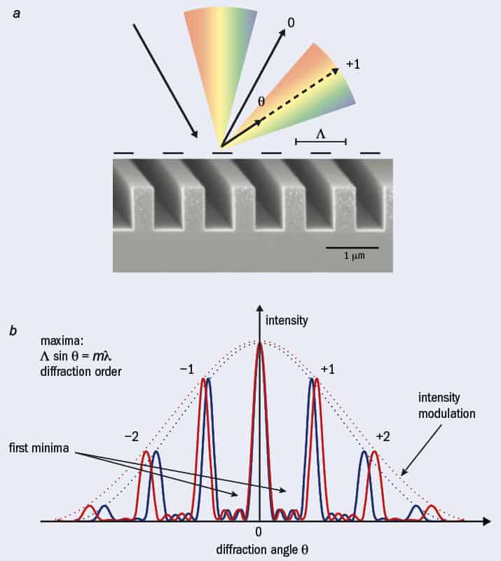
Figure 1: The optical effect of diffraction gratings is based on the interference of light from its periodic elements, leading to the wavelength-dependent enhancement of light at some angles, and the cancellation of electromagnetic radiation at others. (Click for more detail)
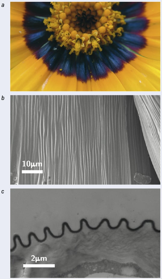
Some flower petals have a particularly interesting example of colour-generating nanostructures. Known as striations, these are parallel surface wrinkles in the petals’ cuticle – the upper wax layer of flowers – and are created when directional growth of the underlying plant cells causes a petal’s surface to physically wrinkle (J. R. Soc. Interface10 20120847). Striations are tiny – barely a few hundred nanometres or 100 times smaller than the diameter of a human hair. Structures on this length scale are similar in size to the wavelength of visible light and therefore they interact with it, causing interference. The interaction is a partial reflection of light at the material interface, caused by light travelling at different speeds when propagating through materials with different optical densities (such as air, water, wax or cellulose). The distance between points where light is reflected determines how light interferes with itself. In particular, the spacing between structure elements dictates which colours are reflected (constructive interference), and which are not (destructive interference).
If floral striations are approximated to a periodic structure, they resemble a diffraction grating (see figure 1). In the first study describing striations, researchers observed a weakly iridescent appearance in a hibiscus and a tulip species, which is typical for relatively ordered gratings (Science323 130). In nature, however, even surface structures that exhibit local order are inherently disordered to some degree. This disorder is seen, for example, in Morpho butterfly wings, where it widens the angular range of the colouration, making the effect visible from more perspectives. Apart from this benefit, however, disorder in (semi-)periodic structures is often seen as an unfortunate and inevitable effect in nature rather than a functional feature.
It’s in the detail
But when our team at the University of Cambridge assessed the role of natural disorder in a dozen flower species with surface striations, we were in for a surprise. We first had to find the flowers with structural colour, which we did by looking at a large number of flowers optically and then with electron microscopy for viewing-angle-dependent coloration (which is evidence for structural colour). The flowers were each selected to be from a different flower family, so they would be only distantly related and span the very large family tree of flowering plants.
Although we first found that the variation in striation size and spacing reduced the rainbow-iridescence drastically, it also gave rise to an unexpected and new optical effect (Nature550 469). While common diffraction gratings reflect all colours relatively equally, but at different angles, the semi-periodic striations on flowers preferably reflect shorter wavelengths (ultraviolet and blue light) in a much wider and more consistent range of directions (at the scattering angle range between about –25 and +25 degrees). We’ve called this optical effect the “blue halo”.
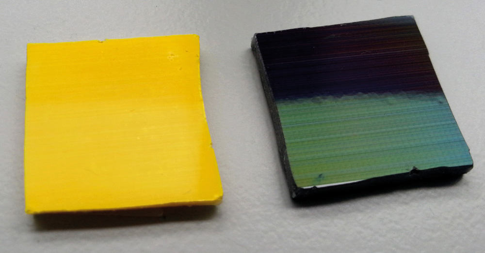
Using computer simulations, we were able to examine different parameters and look at the effects of different feature sizes on this optical halo. Artificially nanostructured samples – made by electron beam lithography and high-resolution flexible mould-based replication – allowed us to confirm the simulation predictions and mimic the optical response of real flowers, while (importantly) making the system less complex. As flowers have so many unique aspects to them, we could not have designed a fair bee-behaviour experiment with real flower samples – the replication method allowed us to make clearly distinct samples that vary only in structuration.
Interestingly, for the different plants analysed, a very similar optical effect was found, despite the height, width and spacing of the striations varying by about a quarter of their size within a flower, and by more than a factor of two between species. Since organization in biological materials is variable, the robustness of the optical effect makes semi-ordered striations particularly useful to achieve a reliable colouration. It also suggests that the amount of disorder in flowers is not random but optimized to some degree. The disorder in floral striations is therefore a functional feature, not a limiting legacy of the structure.
Hidden beauties
Figure 2: The Ursinia speciose exhibits iridescence at the base of its bright yellow petals (click for more detail). (Courtesy: Tobias Wenzel and Edwige Moyroud)
When flowers display a blue halo on a dark-pigmented region, the disordered nanostructure looks blue to the human eye (figure 2) as we cannot see ultraviolet light. The dark underlying layer absorbs the light not reflected by the structure, boosting the contrast and visibility of the structural colour.
Our team was able to identify a dozen very different flowers that had striations, and they all displayed this blue halo effect. However, the structural colour of many of these flowers was hidden from us for a long time, for some because the effect is in the ultraviolet region, which we cannot see, and the underlying pigment does not provide a good contrast to the structural colour. Indeed, in most flowers, bright yellow or red pigment makes it difficult to observe the blue at all.
Of course, the bright colours of flowers have not evolved because they look pretty in a vase on the dinner table. It is irrelevant for flowers whether we humans can see their blue halo or not, but it is vital for most to attract bees because they pollinate flowers and thus secure the plants’ reproduction and evolution.
Bees and bumblebees have a different visual system from humans and therefore they see different colours. For example, instead of the human receptor that enables us to see red colour, bees see ultraviolet light (along with blue and green, which humans also see). By performing behavioural experiments with bees and artificially nanostructured samples that mimic flowers with and without disorder, our collaborators at Cambridge and the Royal Botanic Gardens in Kew, UK, found that bumblebees could see the blue halo well on different coloured backgrounds and identify it quickly. And judging from learning curves and identification speeds, the bees see the optical effect better when the structure is disordered.
The ultraviolet-blue reflectance from striations could therefore be an important evolutionary contribution to the appearance of flowers, especially considering that the plant leaves in the background of flowers are already green (the other colour bees can see), and that blue tends to be a colour that is very difficult to synthesize for most plants.
Multipurpose striations
Copying nature: Artificial epoxy flowers with disordered striations and different background colours (yellow and black). (Courtesy: Tobias Wenzel)
In addition to creating colour, floral striations are likely to have other functions too. Those could include tactile “touch-and-feel” indications for pollinating insects and self-cleaning properties caused by the striations’ enhanced water-repelling properties. Surface striations have also been found in animals, such as beetles, spiders and snakes, where they are likely to perform different functions than in flowers, such as distracting a predator or finding mates.
Our adventure into the details of nanostructures and flower colours has reminded us that we can learn surprising and fascinating engineering principles by looking at examples in nature. The ways in which biological cells produce and organize material sustainably at the nanoscale provides valuable insights to address a number of current challenges in science, technology and everyday life. Nanostructured materials are already used in a wide range of consumer products for manufacturing purposes or device functions, such as sensors that are as sensitive as moth antennae, swimsuits that glide through water as smoothly as sharks do, and surfaces that self-clean away dirt and water just like lotus leaves. Nanoparticles are now used in biology and industry alike to reduce the energy consumption and heat required to form materials.
Could disorder in nanotechnological products provide new functionalities that improve our lives? We might not see biomimetic striations in consumer products any time soon, but the new perspective to obtain functionality from the semi-random variation in nanostructures might inspire future innovation.
For more than 50 years, progress in the electronics industry has been guided by Moore’s law: the idea that the number of transistors in a silicon-based integrated circuit (IC) will double approximately every 18 months. The consequences of this doubling include a continual reduction in the size of silicon ICs, as it becomes possible to provide increasingly complex and high-performance functionality in smaller and smaller areas of silicon, and at progressively lower cost relative to the circuits’ processing power.
Moore’s law is an empirical rule of thumb rather than a robust physical principle, and much has been written about how, why and when it will eventually fail. But even before we reach that point, manufacturers are already finding that, in practice, the cost savings associated with reducing the size, or “footprint”, of ICs will only carry them so far. The reason is that below a certain minimum size, ICs become difficult to handle easily or effectively. For highly complex circuitry, such as that found in computers with many millions of transistors in a single IC, this limit on handling size may not be a consideration. However, for applications that require less complex circuits, the size constraint imposed by the physical aspect of handling ICs becomes a limiting factor in their cost.
This limit matters because as electronics extend further into daily life, there is a growing demand to introduce simple connectivity into everyday items – for example, in tracking and stock control for consumer goods such as milk, shampoo or deodorant that are produced in high volumes with lean supply chains; for interactivity in toys and games; and in “smart” packaging for pharmaceuticals to combat counterfeiting or sense whether medicines have been kept in the optimum temperature range. If we want to maximize the opportunities associated with the so-called “Internet of Things” and extend the range of smart devices beyond high-end consumer goods, then the price point for ICs needs to fall well below that of traditional silicon circuits.
A further factor driving the move away from silicon for low-cost electronics is that regardless of how small silicon ICs get, they are still rigid pieces of material. This makes it difficult to integrate them seamlessly into flexible or curved objects – such as shampoo bottles or juice cartons – without leaving a noticeable bump or impairing the object’s flexibility. Various techniques have been developed to try to correct this, such as covering or encapsulating the IC, but each of these creates challenges of its own as well as additional costs.
The approach we have taken at PragmatIC is to use thin, flexible substrates, rather than rigid silicon, as the base for building our circuits. The low cost of the materials involved and the relatively low complexity of our target applications alters the economics around circuit footprint and overall IC cost. Accepting a larger footprint can lower capital expenditure because it means that ultrahigh-end precision tooling is not required to fabricate our circuits during the manufacturing process. In turn, for low-complexity applications, this can lead to a lower final IC cost.
The resulting flexible integrated circuits, or FlexICs, are thinner than a human hair, so they can easily be embedded in everyday objects. They also cost around 10 times less than silicon ICs, making it economically viable for them to appear in trillions of smart objects that engage with consumers and their environments. Since the technology was developed, PragmatIC FlexICs have been trialled in a wide variety of markets, including consumer goods, games, retail, and the pharmaceutical and security sectors.
In addition to the circuits themselves, PragmatIC has also developed a compact, automated system to manufacture FlexICs at high volumes. Whereas a conventional silicon IC fabrication facility, or “fab”, would typically require billions of dollars in upfront capital investment (not to mention considerable time) to set up, PragmatIC’s FlexLogIC™ “fab-in-a-box” model costs several orders of magnitude less and offers a greatly shortened build time. This system is also significantly smaller than a conventional silicon fab, and its self-contained nature makes it possible to install it in a wide range of manufacturing environments, such as label and packaging facilities.
We believe that this system has the potential to transform the market for flexible electronic solutions, as it enables non-electronics companies to become part of the supply chain. Because the FlexLogIC system is fully automated, it can be operated by companies with comparatively low levels of electronics expertise. The upfront design costs are also considerably lower, so new flexible electronic solutions can be developed, tested and rolled out in weeks (or eventually even in days) rather than months, and with reduced risk. This reduction in both cost and time enables a scalable distributed production model. Compared with silicon ICs, where a few huge foundry companies produce most of the world’s supply, the FlexLogIC model can support a large number of global manufacturers, across multiple locations.
The resulting flexible integrated circuits, or FlexICs, are thinner than a human hair, so they can easily be embedded in everyday objects; and they cost around 10 times less than silicon ICs
Model differences
Whenever you try to bring new technologies and products to the mass market there are always challenges, and the products discussed above are no exception. In our experience, one of the ways to overcome these hurdles – perhaps a bit counterintuitively for a hi-tech industry that thrives on innovation – is to avoid adding novelty unless it is absolutely necessary.
As an example, we have found that using off-the-shelf equipment and components wherever possible is a must. Anything bespoke immediately introduces challenges. There will be additional upfront costs. The level of maintenance support from the manufacturer will not be the same as with standard tools, and it will be more difficult to find and hire knowledgeable production staff who have used similar tools before.
The mantra of “novelty only where needed” also stretches back to the design phase, where the underlying physics of our devices has a direct impact on the assumptions we use to simulate their behaviour. PragmatIC uses devices built on metal oxide semiconductors, where charge carriers move via band conduction in spherically symmetric s-orbitals with a high degree of spatial overlap. This differs significantly from conduction in silicon, where there is strong spatial directivity in the sp3 orbitals that control the conduction pathways. One implication of this difference is that, whereas any disruption of silicon’s ordered lattice will significantly impair the mobility of charge carriers, the high degree of orbital overlap in metal oxides means that carrier mobility is not sensitive to the film structure in the same way.
This presented us with a conundrum. We had selected commercial circuit design tools because they are well supported, regularly updated and familiar for external users. However, commercially available design tools predominantly use well established silicon-based models to predict and describe how IC devices will behave, and unfortunately, we found that these models did not fully describe the physics of our devices. For example, in crystalline silicon transistors, an increase in temperature will reduce the mobility of charge carriers in the transistor, but in amorphous oxide transistors the mobility will actually increase with temperature. Consequently, we had to work out how our devices’ behaviours differed before we could understand where the models were likely to be accurate, and where they were not.
Once we had got to grips with the limitations of our models, we had to do some additional work to avoid building inconsistencies between the model device and the real one into our simulations. Some of this work was theory-based, but there was also a lot of experimentation: PragmatIC builds from the ground up and evaluates devices in different scenarios to understand how performance compares with the predictions from the models. This informs slightly more complex circuitry, which is then evaluated in the same way and so on in an iterative process. In 20 or 30 years, theoretical models based on metal-oxide semiconductors may have evolved to the point where we can avoid this kind of trial-and-error work, but right now, the highly developed models that exist for silicon are simply not available for our system.
The right approach
There are usually one or two key differentiators that make a product unique and could create opportunities in the market. However, the typical consumer will not be interested in how this unique product is made, only in its final functionality. Although it is always more stimulating on a personal or intellectual level to be trying something new and figuring out how to get it to work, if your exciting new technique will increase costs without augmenting the functionality, then it is a commercial non-starter. Hence, unless a new approach actually provides a commercial advantage, it should not be pursued, no matter how innovative it is.
By the same token, we know that flexible electronics will not replace silicon electronics in areas where silicon excels. In terms of actual computing, there is nothing our technology can do that silicon cannot. However, in areas where silicon falls down, a new approach overcomes the commercial disadvantages of doing things differently – and thus offers a route to new implementations of electronics in everyday household items that have not, until now, been economically viable.
Two new technologies that use laser frequency combs to detect natural gas leaks have been unveiled by independent teams of researchers in Boulder, Colorado, US.
Gas leaks are a significant problem for the energy industry. As well as costing money, leaks pose serious threats to safety, public health and air quality. Methane – the main component of natural gas – is also a potent greenhouse gas.
Now, Nima Nader and colleagues at National Institute of Standards and Technology (NIST) in Boulder have created a new laser-on-a-chip that can be used to detect gas leaks. Meanwhile at the University of Colorado Boulder, Gregory Rieker and colleagues have created an infrared spectroscopy system that can detect small amounts of methane at kilometre distances.
Detection challenges
While there are several techniques available for monitoring facilities for gas leaks, all have shortcomings. One method involves using specialized cameras that are sensitive to methane at short distances. However, this monitoring process is labour intensive and does not give a comprehensive image of leaks over large areas. Alternatively, images from aircraft or satellites can reveal multiple large leaks over distance scales of kilometres – but show little detail of smaller leaks. Another problem with aerial and satellite images is that they provide snapshots in time, rather than continuous monitoring.
Now, Nader and colleagues at NIST have developed a new chip-based source of mid-infrared laser light that could form part of a practical system to detect gas leaks. Mid-infrared light is absorbed by many organic molecules including methane and analysing the absorption spectra of air that the light has passed through reveals the presence of these molecules. However, mid-infrared spectroscopy currently suffers from a shortage of broadband light sources, high levels of noise and high power requirements.
Silicon-on-sapphire
To address these shortcomings, Nader’s team have created the first mid-infrared “dual-frequency combs” on a chip. To create the lasers, the researchers carefully engineered the geometry and chemical composition of a silicon-on-sapphire waveguide that fits on a chip of just 1 cm².
Dual-frequency combs are low-power laser sources that generate two coherent beams. Each “tooth” of the laser is a narrow peak of light at a specific frequency and the teeth are spread over a wide range of frequencies, with little noise. The spectral nature of the light can be tuned so that the system can be used to study different molecules.
“The laser source enables long-distance propagation of light so chemical samples can be studied remotely, without direct contact,” explains Nader. “Since frequency combs are stabilized laser sources, they can detect very low levels of chemicals and enhance the sensitivity of our measurements.”
Pinpointing leaks
Elsewhere in Boulder, the University of Colorado team is the first to deploy a mid-infrared, dual frequency comb laser spectrometer in the field. Their ultimate plan is to create a monitoring system in which many laser sources are strategically arranged across a gas production site, all pointing towards a mid-infrared spectrometer at the centre of the facility. When coupled with atmospheric models, absorptions in the dual-frequency comb spectra resulting from leaked gas crossing the beam paths would provide a sensitive measure of gas concentrations over time. Furthermore, the distributed nature of the system could pinpoint the location of a leak.
The team has done preliminary tests of their detection system, which the researcher say has significant advantages over existing methods of monitoring gas production sites. Rieker explains, “Our approach allows measurements to be autonomous, which enables continual monitoring of an area”. Importantly, the system is sensitive to small changes in the concentrations of both methane and water vapour. “The change in methane concentration downwind from a small leak is about the same as the change in methane due to dilution by water vapour that occurs when a rainstorm starts,” Rieker explains. “Laser frequency comb spectroscopy allows us to simultaneously, and accurately, measure water vapour and methane. This lets us correct for water in the air, which is critical for detecting very small increases in methane over a large area.”
The University of Colorado researchers carried out two field tests with their setup. The first exercise simulated a small, time-variable methane leak, situated over a kilometre away from a laser source. The system detected the leak, which released 1.6-8 g of methane per minute. This rate of release is comparable to the rate at which a human exhales air while breathing normally. In the second test, a network of beams was set up to monitor a gas production field with five potential leak sites. Again, the setup accurately measured two simulated leaks simultaneously, while accurately pinpointing their locations. Following the success of their demonstration, the team hopes their system will soon be available commercially.
The University of Colorado study is described in Optica and the NIST research is described in APL Photonics.
Artificial intelligence (AI) technology holds much promise for improving the quality of healthcare, but there are crucial ethical issues that need to be considered for the benefits of machine learning to be realized, according to a perspective piece published in the New England Journal of Medicine (N. Engl. J. Med. 378 981).
Implementation of AI in healthcare requires addressing ethical challenges such as the potential for unethical or cheating algorithms, algorithms trained with incomplete or biased data, a lack of understanding of the limitations or extent of algorithms, and the effect of AI on the fundamental fiduciary relationship between physicians and patients, according to a Stanford University team led by Danton Char.
All of these issues are also relevant to radiology, said Char, who is an assistant director at Stanford’s Center for Biomedical Informatics Research and co-director of Spectrum, a research centre funded by a US National Institutes of Health (NIH) Clinical and Translational Science Award.
Unethical, cheating algorithms?
AI algorithms could be designed to perform in unethical ways – as evidenced in nonhealthcare examples such as Uber’s Greyball algorithm for predicting which potential passengers might be undercover law-enforcement officers. Algorithms can also be developed to cheat, such as when Volkswagen’s algorithm enabled vehicles to pass emission tests by reducing nitrogen oxide emissions during tests.
Similarly, developers of AI for healthcare applications may have values that are not always aligned with the values of clinicians, according to Char and Stanford colleagues Nigam Shah and David Magnus.
There may be temptation, for example, to guide systems toward clinical actions that would improve quality metrics but not necessarily patient care. Or these algorithms may be able to skew data provided for public evaluation when being reviewed by potential hospital regulators, according to the authors.
It’s also possible to program clinical decision-support systems in a manner that would generate increased profits for their designers or purchasers, such as by recommending tests, drugs, or devices in which they hold a stake, or by altering referral patterns.
“The motivations of profit versus best patient outcomes may at times conflict,” Char told AuntMinnie.com.
This perpetual tension of generating profit versus improving patient health must be addressed, because the developers and purchasers of machine-learning systems are unlikely to be the ones delivering bedside care, according to Char and colleagues.
Another issue is the danger of self-fulfilling prophecies. The underlying data used to train an algorithm can be incomplete or biased, and the functioning algorithm may then reflect these biases.
“If clinicians always withdraw care in patients with certain findings (extreme prematurity or a brain injury, for example), machine-learning systems may conclude that such findings are always fatal,” the authors wrote. “On the other hand, it’s also possible that machine learning, when properly deployed, could help resolve disparities in healthcare delivery if algorithms could be built to compensate for known biases or identify areas of needed research.”
Blind faith or scepticism
In addition, physicians don’t understand the limitations or extent of AI algorithms, creating the potential for blind faith or scepticism.
“Treating them as black boxes may lead physicians to over-rely or under-rely on AI systems,” Char said.
The authors noted, though, that physicians who use machine-learning systems can become more educated about how these algorithms are constructed, the datasets they were trained from, and their limitations.
“Remaining ignorant about the construction of machine-learning systems or allowing them to be constructed as black boxes could lead to ethically problematic outcomes,” they wrote.
Fiduciary relationship
AI also changes the dyadic, fiduciary relationship between the physician and the patient – a relationship that has already been shifting in clinical medicine to one between a patient and an electronic health record system, Char said.
“Things like privacy are already difficult to guarantee,” he said. “Implementing AI systems takes these [concerns] even further. What role and ethical duties do these autonomous systems have in the fiduciary relationship between a patient and their provider?”
With AI, the relationship will now be between the patient and the health system, according to the authors. Consequently, the adoption of machine-learning systems will require a reimagining of confidentiality and other core tenets of professional ethics.
“What’s more, a learning healthcare system will have agency, which will also need to be factored into ethical considerations surrounding patient care,” they wrote.
Ensuring ethical standards
The authors believe that the potential for bias and questions about the fiduciary relationship between patients and machine-learning systems are challenges that need to be addressed as soon as possible.
“Machine-learning systems could be built to reflect the ethical standards that have guided other actors in healthcare – and could be held to those standards,” they concluded. “A key step will be determining how to ensure that they are – whether by means of policy enactment, programming approaches, task-force work, or a combination of these strategies.”
A new biocompatible material that stiffens when it is stretched and changes colour in the process might be used to make better medical implants among other potential devices. The material, which is made from mouldable elastomers through the self-assembly of “bottlebrush” copolymers, mimics the way biological tissue behaves and is the first to combine both strain adaptive stiffening and colour change in one material.
Biological tissues show complex mechanical and optical responses that are difficult to replicate in synthetic materials. For example, skin protects the body by, for one, rapidly stiffening to prevent injury. Some organisms, such as chameleons, cephalopods and amphibians, can even change the colour of their skin in certain situations. Chameleons rapidly go from a “cryptic” (or camouflage) state, for instance, and an excited state (mainly exhibited during courtship or combat).
Researchers from the US, France and Russia led by Sergei Sheiko of the University of North Carolina at Chapel Hill, and Andrey Dobrynin of the University of Akron, Ohio, have fabricated the first chameleon-inspired elastomers that boast both strain adaptive stiffening and colour-change behaviour. They made the materials by synthesizing triblock copolymers comprising linear ends and a central block resembling a bottlebrush in which the side chains extend like bristles from a linear chain backbone. “The central bottlebrush block forms a soft matrix and the linear end chains self-assemble into rigid domains playing the role of multifunctional physical cross-links,” explains Dobrynin.
This special combination produces a rigid-while-flexible and soft-while-stiff material that has a low Young’s modulus. The fact that the two chemically dissimilar blocks are separated by microphases also improves its strain-stiffening characteristics so that it is on a par with that of skin tissue.
Synthetic pig skin
By carefully selecting the length or density of the bottlebrush’s side chains, the researchers found that they were able to control how the material is deformed. They even succeeded in “coding” in all the parameters required for it to exhibit a mechanical response that was identical to that of living tissue. For example, they produced mouldable elastomers with strain-stiffening characteristics close to those of lung, brain, skin and blood vessel tissue. “These materials are solvent free, could have mechanical properties similar to pig skin, do not dry out in air or swell in bodily fluids,” says Dobrynin.
Being able to tune the mechanical properties of a material in this way could be useful for making biological devices, such as intervertebral discs, for example, that have mechanical properties similar to those of surrounding tissue to minimize the inflammatory response, he adds.
Microphase-separated structure
Importantly, the material also changes colour when it is deformed. Thanks to atomic force microscopy and X-ray diffraction measurements, the researchers discovered that the terminal blocks of the polymers self-assemble in nanometre-sized spheres. Light interferes with the microphase-separated structure and the colour observed depends on the distance (or gap) between the spheres. This is very much like what occurs in photonic crystals, nanostructured materials in which the periodic variation of the refractive index on the length scale of visible light produces a “photonic bandgap”. When the material is stretched – that is, the distance between the spheres is increased – the colour reflected goes from turquoise to dark blue.
The team, which also includes researchers from the ESRF in Grenoble, the University of Haute Alsace, the Institute of Materials Sciences in Mulhouse and Moscow State University, detail their work in Science DOI: 10.1126/science.aar5308.
The time lag before increasing carbon dioxide levels for El Niños originating in the eastern tropical Pacific is about 8.5 months, the researchers say, whereas the lag for El Niños starting in the central tropical Pacific is about 5.2 months. However, the sensitivity of carbon dioxide rise to tropical near-surface air temperatures is similar for each type of El Niño.
The results should enable scientists to better constrain the effects of El Niños in climate models.
“The time lag can be used to form a reasonable hypothesis about the way vegetation reacts to the El Niño effects,” said Petr Chylek of Los Alamos National Laboratory, US.
It is common knowledge that climate is affected by atmospheric carbon dioxide concentrations, but what can be less obvious is how carbon dioxide is affected by the climate. When it comes to El Niños, the important factors are the absorption of carbon dioxide by the oceans and by vegetation.
An El Niño results from a warm ocean, which is less able to absorb carbon dioxide than a cold one; what’s more, an El Niño has the potential to cause droughts in some regions, either inducing wildfires or restricting the growth of vegetation, so limiting its capacity to photosynthesize.
The overall effect is that any El Niño leads to a delayed rise in carbon dioxide – although “most experts are of an opinion that the vegetation effect probably dominates,” said Chylek.
The resulting rise in carbon dioxide is usually between one and two parts per million – roughly the same as the overall annual rise in the gas – and is short-lived, lasting about a year. Nevertheless, understanding its dynamics is important for fine-tuning climate models.
Chylek and coworkers analysed historical data on tropical near-surface air temperatures from the University of Alabama, US, and carbon dioxide levels from the Mauna Loa Observatory in Hawaii, for the years 1960–2016. As expected, they found that each peak in temperature was followed by an increase in carbon dioxide, although the time lag was different depending on the El Niño origin.
The researchers suspect the reason El Niños originating in the central tropical Pacific have a smaller time lag is they can be linked to wildfires, whereas El Niños originating in the eastern tropical Pacific can be linked to changes in vegetative respiration. “Future research will confirm or reject our hypothesis,” they said.
The team, which published the study in Environmental Research Letters (ERL), now plans to follow the paths taken by El Niños in terms of their changing precipitation, to see from satellite data the effect on vegetation.
Physics is at the heart of innovations all around us. From laptops to sat-navs and mobiles, it’s in your home, in your car and in your pocket. Physics helps you get more work done and enjoy more time off, gets you where you’re going, and keeps you safe. It underpins the growth that will secure our economic future. We as physicists know that, but does the rest of the world?
There are many definitions of innovation in business, but perhaps the simplest – and the one that sticks most in my mind – is attributed to Geoffrey Nicholson, the father of the Post-it Note. While working at the US adhesives giant 3M, he is alleged to have said: “Research is the transformation of money into knowledge; innovation is the transformation of knowledge into money.” It’s a simple enough statement, but doing innovation, and succeeding commercially at it, that’s the difficult bit.
As I mentioned in my first Transactions column, my career in industry has in some ways been quite specialized and left me unaware of all the amazing things going on in the wider physics community. However, during my stint as vice-president for business at the Institute of Physics (IOP), which publishes Physics World, I have had the good fortune to serve on the judging panel for the IOP’s business innovation awards. Running since 2012, they have showcased some of the fantastic and wide-ranging innovations created by entrepreneurs using physics.
The awards are the only ones to recognize companies in the UK and Ireland that have built success on the innovative application of physics. These are the businesses that have generated profit, secured jobs and improved efficiency across a range of sectors. Looking at last year’s nine winners, they are an impressive bunch covering medicine, cryogenics, microscopy, imaging, solar cells, space technology, communications, advanced generators and shock testing.
One of the challenges facing physics-based businesses is how much longer it takes to develop products or services compared to, say, a chef who wants to open a restaurant. It can take years to get products ready and usually requires significant investment. There is also the added challenge of explaining the physics of a product idea, which is often quite specialized, to financial investors or business angels with little or no scientific knowledge.
Physics-based firms can take years to get products ready and usually requires significant investment. There is also the added challenge of explaining the physics of a product idea
There have been many occasions when I’ve had to bite my lip when a confused investor tries to paraphrase my in-depth pitch about the technology with a comment like “Oh so what you mean is…” What you want to say in reply is something like, “Er no, that’s completely wrong. I can see you didn’t get it or weren’t listening.” Instead, a diplomatic “Well, yes, it is a little like that, but…” emerges from your lips.
A kick-start for start-ups
Recognizing that small firms face their own, unique challenges, my colleagues and I at the IOP have decided to split the business innovation awards so there are now separate business start-up awards. Previously it had been hard for an early-stage business to provide sufficient evidence of commercial growth to be recognized. (There are also IOP awards for people and teams who have applied physics in a commercial or industrial context, namely the Katharine Burr Blodgett, Denis Gabor and Clifford Paterson medals and prizes.)
For small businesses, winning one of the new start-up awards from the IOP would be a serious risk-reduction factor for potential investors. It would be a sign that the company’s physics and technology have been examined by an expert judging panel of serious and experienced physicists. With the IOP’s stamp of approval on your technology, persuading someone to plough their money into your business would suddenly be a whole lot easier.
I can imagine a conversation with an investor running something like:
“Well our product is based on this principle and we recently won an IOP start-up award.”
“Oh, that’s interesting. Tell me about that…”
The start-up award is, if you like, a quality seal for your product and validates that the physics and its implementation is sound and that the business concept has merit. Apart from improving the confidence that future investors and customers will have in your company and product, the award could also pave the way for future funding, give you constructive feedback from seasoned business leaders on the judging panel, and raise the profile of your firm and its products.
The meaning of success
Dyed-in-the-wool academics might find all this talk about profile-raising and marketing a little grubby, but it’s true that if no-one knows about your technological innovation, no-one will buy it or buy into it. So the opportunity to showcase your product at a reception in the Houses of Parliament, as the IOP innovation-award winners get to do, is an invaluable way for you to network with funding agencies, senior industrialists and politicians.
The winning firms are also invited to the IOP awards dinner, get highlighted on the IOP’s marketing and social media, get to speak at relevant IOP meetings, and take part in our new business innovation and growth group. Now, none of this will guarantee that everything else will work out, as there are many other hurdles to jump over to reach that nirvana state of “successful”, which in itself takes on many forms. Should you judge a business’s success in terms of its growth, turnover, exports, profits or social impact?
Like beauty, commercial success is in the eye of the beholder. But an IOP start-up award will certainly help.
The closing date for entering this year’s IOP business innovation awards is 18 May – see here for more details.
We’re always hearing about how graphene is going to revolutionize this or that. Has progress in research and commercialization been as quick as you’d anticipated?
I think so, because if you look at any major technology based on hardware, as opposed to software, it has always taken between 20 and 40 years to go from the initial discovery to mass applications. The first transistor was in 1947, but it took more than 10 years for people to realize that they had to use silicon instead of germanium. Or if you take carbon fibre, the first time anyone put carbon fibre in a car was in the earl 1980s, but the first commercial fully carbon-fibre car only happened in 2013. Any new “node” technology requires several years to develop and massive investments of (at least) $10bn, and that is just for one node.
So yes, it’s completely normal to expect a 20- to 40-year time frame. What is not normal is that the media has built up an expectation around graphene that is clearly not possible. It’s similar to when the government announces that there will be a high-speed rail link between two towns, and after two months people ask, “Where’s the train?” It clearly doesn’t work like that. From my point of view, we are perfectly on track over a 20- to 40-year roadmap for graphene applications.
What will those first applications be?
The first applications are already here, and they are related to inks, coatings and polymer composites. There are skis, tennis rackets and cars with graphene in them that you can buy, and masks with graphene filters for working in the lab. I mean, there’s lots of things you can buy already that are made with graphene. Even underwear.
Graphene underwear?
Yes, you can buy graphene underwear – there’s a company in China producing it. There are many, many products out there. If you want a motorcycle helmet with graphene, you can already buy that. You can buy shoes that have graphene inside. These products are not particularly hi-tech and they mostly rely on graphene’s thermal properties, maybe antibacterial properties, and mechanical properties. These are the low-hanging fruits and we now have a plethora of start-up companies in the UK and also in Europe making graphene inks, composites, paints and powders.
But then you start to think about creating consumer electronics – optoelectronics, photoelectronics – with graphene, and this will require massive investment. We’re talking about 10 or 20 years before we can really implement these. Yet the more it goes forward, the more I start to believe that the technology will succeed. I cannot tell you if it’s going to be a million-, billion- or trillion-dollar market, but for a million-dollar market we are already there – it already exists.
These great investments that are needed over the next couple of decades – what do they need to address?
The investment required is of a similar order of magnitude to what you need nowadays to develop a new silicon-based device. We are talking about hundreds of millions to develop a technology that is ready for mass production. But you can also have much lower investment in the form of pump-priming to help companies test proof-of-principle devices.
So is the money going into designing and building new fabrication facilities?
No, the idea at the moment is to integrate graphene with existing silicon CMOS fabs. Of course, there are new tools being developed, but essentially these are chemical vapour deposition tools, so they are very similar to the tools that you already have in the fab. What you really need to develop is the process – the temperature, the chemicals and also things like the fact that at the moment graphene is often grown on copper foil, which is forbidden in silicon fabs because of contamination. You can use iron chloride to remove the copper, but then you get iron contamination. So one direction is to try to grow graphene directly onto silicon – this is very complex, but probably feasible.
We are entering a phase where a lot of things that are not so important when you write a paper for a scientific publication are becoming crucial. If you want to develop this technology, you need to optimize the material to meet the key performance indicators, such as electron mobility and scattering time, that will really make graphene much better than the current technology on the market – and you need to do it in a way that will work on a mass scale. In the lab, we have already shown that graphene is much better than the current technology. But clearly, a laboratory device doesn’t face all the problems that you get when you need to scale up the device and integrate it with other systems.
Layers upon layers: Molybdenum disulphide is one of several 2D materials with possible technological applications.
Where do other 2D materials fit into this picture?
I would actually call them layered materials, because while graphene is certainly a monolayer of atoms, for something like molybdenum disulphide (MoS2) the “one layer” is actually three layers: one of molybdenum and two of sulphur. So it’s a bit of a stretch calling them 2D, even though, clearly, they are more 2D than 3D. There are about 2000 of these materials that we know of and very few – probably 10 or 15, although I don’t know the exact number – have been studied so far. Of course, people have studied many of them in bulk form, but you have to exfoliate them to get the monolayer, and when you do that, the material’s properties change. The other thing is that even with graphene, when you stack a layer of graphene on top of another layer, you can go from a metal to a semiconductor just by changing the angle between the layers. The same thing happens with all the other materials, and when you put them together – say graphene, boron nitride (BN) and MoS2 – that creates yet another spatial option. And then you can twist them, and so on.
So, in terms of research options, we have plenty of materials to study for the next 100 years. From the applications point of view, though, clearly graphene has come much further than the others because work on it started earlier. So when we speak of applications, graphene is going to be the first. After that, other materials that are now reaching maturity include BN (as a nice substrate or a way of encapsulating graphene), MoS2, and tungsten diselenide or tungsten disulphide (WS2). These materials are getting closer to the application stage and if you are interested in light-emitting diodes or even transistors, they are better than graphene because they have a band gap and graphene does not.
These other 2000 materials – you say they haven’t been studied yet, not because they aren’t promising, but just because we haven’t got around to it?
Just because we don’t have 200 million PhD students, yes. It should also be said that until two years ago, nobody bothered to classify these layered materials. Now, several theoretical groups have used data-mining techniques to search the crystallographic databases for layered materials, and they have established that there are between 1500 and 2500 of them – it’s not even clear what the precise number is. There are also at least 80 other materials that are three-dimensional but can be made layered; you start from a covalently bonded material that you would not think could be exfoliated, but then you do some tricks and it becomes possible.
So, really, this idea of graphene has uncovered a completely new field of research. Almost every week there’s something new coming up. But from my point of view, at this moment I would rather take graphene and WS2 and BN and so on – these few materials that are well known – and really push them forward technologically. I think new groups may have a bigger incentive to go and explore random materials because I am pretty sure that at some point somebody will find a material we don’t know about that has much better properties than graphene and the others. But we can’t keep looking for the new ones if we are interested in applications.




 Artificial intelligence (AI) technology holds much promise for improving the quality of healthcare, but there are crucial ethical issues that need to be considered for the benefits of machine learning to be realized, according to a perspective piece published in the New England Journal of Medicine (