Twisted light controlled by metasurfaces

Researchers in the US have created metasurfaces that can switch the orbital angular momentum (OAM) of transmitted light between any two states simply by changing the polarization of light incident on the materials. The metasurfaces offer a simple and practical way to produce “twisted light” with OAM, which has a range of applications from the mechanical manipulation of tiny objects to quantum communications.

The angular momentum of light is the sum of two independent components. One is the more familiar spin angular momentum (SAM) associated with circularly polarized light. It arises from the electric and magnetic field vectors of light rotating over the course of a wavelength. SAM can be produced easily by firing plane polarized light through a crystal slab called a quarter wave plate. However, SAM is of limited practical use because it can only have two values – right or left circular polarization.

OAM of light was first measured in 1992 and is the result of the rotation (or twisting) of a light wave’s phase around the axis of a beam. In principle, OAM can take any integer value and this makes it very useful for a wide range of potential applications. It can be used, for example, to trap tiny particles and set them rotating at a very fast rate in a device called an “optical spanner”. In addition, as waves with different OAM are orthogonal, researchers are already developing ways that light in different OAM states can be used to send an unlimited number of multiplexed data signals along an optical fibre with no crosstalk.

Challenging production

Producing OAM states, however, is challenging. Various techniques exist, but their efficiency – the proportion of the light that is converted into the desired angular momentum state – is sometimes limited, and they do not allow easy switching between different angular momentum states, which would be necessary for multiplexing, for example.

In 2006, the optical physicist Lorenzo Marrucci of the University of Naples Federico II in Italy and colleagues designed a device called a q-plate, which flips the polarization of incident light. During this process SAM is removed from the light and transformed into OAM. Q-plates channel light into the correct OAM state, with up to 100% efficiency, and the state can be changed simply by flipping the SAM of the incident beam. However, q-plates only work with pure right or left circularly polarized light, whereas light beams often have intermediate “elliptical polarization”. Moreover, they can produce only two possible output states: a fixed amount of OAM is added to one spin state; an equal and opposite amount is added to the other spin state.

Federico Capasso and colleagues at Harvard University in the US worked out the most general mathematically possible transformation a surface could perform from two input polarizations to two output OAM states. “It turns out no traditional material can produce this required effect,” says Harvard’s Robert Devlin. Therefore, the researchers designed artificial metasurfaces comprising thousands of nanometre-scale titanium oxide pillars. The metasurface can be designed such that any two equal and opposite input polarization states are each transmitted into any output OAM states whatsoever.

Working on the beam

The total angular momentum of the beam need not be conserved because the metasurface can do work on the beam. “If we had a really, really small device and a very intense beam coming in then, for all of these cases where there isn’t a perfect transfer from spin to orbital angular momentum, you would actually see the device itself start to spin,” explains Devlin. This can allow the production of states with output OAM greater than the limit quantum mechanics places on the input SAM.

Previously, similar transformations would have entailed passing light through several optical components in succession: “Now that the device has been distilled down to a single component, rather than eight or so elements on an optical table, one can directly integrate the single device into a variety of areas, and there is the potential for new experiments and applications in communications and quantum optics,” says Devlin. “Where it ultimately goes, what it ultimately gets used for and whether it enables some completely new functionality – that’s the exciting part that we’re exploring now.”

Marrucci, who was not involved in the research, is enthusiastic: “Metamaterials have been around for a while, but most of the work was with plasmonic metals, which are lossy and hence not so convenient,” he says, “I think the main advance here is to demonstrate what can be done with dielectric metamaterials. This specific demonstration of arbitrary spin to orbital angular momentum conversion shows they can do something not easily done with different technologies. I wouldn’t say this specific optical effect is particularly important fundamentally, but the paper brilliantly demonstrates the huge potential of this novel technology,” he says.

The research is described in Science

Giving scientific advice in Japan

By Michael Banks in Tokyo, Japan

US President Donald Trump might be in Japan right now eating hamburgers and playing golf with the recently re-elected prime minister Shinzo Abe, but his presence didn’t stop me and Physics World editor Matin Durrani having our own high-level meeting as we began our week-long tour of the country.

After landing at Haneda airport in Tokyo, we headed straight to our downtown hotel for a meeting with Tateo Arimoto, who is director of science, technology and innovation at the National Graduate Institute for Policy Studies and a principal fellow of the Japan Science and Technology Agency (JST).

Over a light dinner of sushi, rice and vegetables, we had a wide-ranging and frank discussion about the role of scientific advice in Japan.

Arimoto, who has had a 40-year career in Japanese science-policy circles, noted that before the deadly earthquake and tsunami that hit Japan in 2011, scientific advice to the Japanese government was fragmented. Back then, there was no clear mechanism for giving scientific advice to the government, which proved problematic when quick action was needed after the Fukushima nuclear plant was hit. Science advisers are common in other leading scientific nations, notably the UK and the US (though Trump has still not appointed anyone to the role, almost 10 months after taking office). But no such position existed in Japan.

“Following Fukushima, the government wasn’t able to call on an appropriate mechanism for advice and analysis,” says Arimoto.

Japan has since gone on to set up the Council for Science, Technology and Innovation, which is chaired by prime minister Abe. Yet the council, which meets every month, mostly focuses on how to boost innovation in Japan, with many of its panel members being leading figures from industry. A single science adviser still does not exist.

In 2015 Japan’s foreign ministry became the first government body to appoint a dedicated science adviser, which Arimoto says was “a very important move”.

The first person to hold the position, which changes hands every two years, is the materials scientist Teruo Kishi from the University of Tokyo who is a former president of the National Institute for Materials Science. “The JST is supporting Kishi in this role,” says Arimoto. “But we need more help.”

So does Japan need a central figure to give science advice to the prime minister? Arimoto was coy about giving a straight answer, noting that whether it is better to have a single person or a panel depends on the national system as well as cultural aspects.

My hunch is that Arimoto is in favour of the Japanese government appointing a chief scientific adviser.

Indeed, he pointed to the impact that John Beddington, who was the UK’s chief scientific adviser from 2008 to 2013, had in the immediate aftermath of the Fukushima incident.  Whereas France chose to move its citizens out of Tokyo, despite the Fukushima plant being 300 km to the north of the capital, Beddington’s advice to the UK embassy was that such drastic action for UK nationals in the country was not necessary. “That quick decision alone helped stabilize the situation in Japan,” Arimoto admits. As he wrote in a fascinating article last year, Beddington’s advice not only helped British and Japanese people, “It created positive impacts on Anglo–Japanese diplomatic relations”. If Trump wants to boost US–Japanese links, perhaps he should not waste any more time without his own science adviser.

Once our dinner was over, Arimoto headed straight to the airport to attend the World Science Forum in Amman, Jordan where he will be talking about rebuilding broken societies through reconstruction.

Konnichiwa Japan

By Michael Banks

Suitcases packed, Matin Durrani and I will be travelling to Japan over the weekend for a week-long road trip that will see us heading to Tokyo, Osaka, Kyoto and Kamioka.

It’s a busy schedule that includes meeting with senior policy-makers and visiting a number of high-profile institutes.

The main purpose of our visit is to gather material for a special report on Japan that will be published in February 2018 (for this year’s reports on China and the US see here and here).

The packed itinerary includes the RIKEN laboratory in Wako, the Super Kamiokande neutrino detector in Kamioka as well as the Kavli Institute of Physics and Mathematics of the Universe and the Earth Life Science Institute, both of which are in Tokyo.

We will be meeting with Hikaru Kawamura, president of the Japanese Physical Society, as well as senior officials from the Japan Society for the Promotion of Science and Japan’s Council for Science, Technology and Innovation.

And that isn’t all – we will also fit in a seminar on science communication at Tokyo Institute of Technology.

So make sure you keep an eye out on the blog for regular updates about our trip.

Putting a stamp on gravitational waves, LEGO’s Women of Nasa, physicist competes in bake-off

By Michael Banks and Hamish Johnston

For those wanting to add a physics twist to your season’s greetings, you now can thanks to Germany’s Federal Ministry of Finance. It has announced two new stamps that will go on sale in the country on 7 December. A €0.40 stamp will feature the European Space Agency’s Gaia satellite and will be the first German stamp to include a metallic coating. Gaia was launched in 2013 to measure the positions and distances of astronomical objects, including stars, planets as well as comets. The ministry also announced a €0.70 stamp that depicts the gravitational waves that emerge from the collision of two black holes. The simulation was made by researchers at the Albert Einstein Institute (AEI) in Potsdam, Germany. “The ministry did not announce whether letters equipped with the new gravitational-wave stamp will be transported at the speed of light,” states an AEI press release.

LEGO in space: the "Women of NASA" kit (Courtesy: LEGO)

Are you looking for a NASA-themed present for someone who is crazy about space? We can recommend LEGO’s “Women of Nasa” building kit, which features minifigures of four women who have made major contributions to the agency. These include NASA executive and “Mother of Hubble” Nancy Roman, who pioneered space astronomy; and the computer scientist Margaret Hamilton, who led the development of the on-board flight software for NASA’s Apollo Moon missions. Also in the kit are the astronauts Sally Ride, who was the first American woman in space and Mae Jemison, the first African-American woman in space.

Physicist baker: James Hoyland on The Great Canadian Baking Show (Courtesy: CBC)

Earlier this year Physics World visited the physicist Nathan Myrvold at his “cooking lab” in Seattle and learned just about everything one would ever want to know about “The physics of bread”. Elsewhere in the Pacific Northwest, the Vancouver-based physicist James Hoyland is competing on The Great Canadian Baking Show, which premiered Wednesday on CBC. Originally from Darlington in north-east England, Hoyland told the Metro newspaper, “I’m still an experimental person – there’s physics and chemistry as well. People say cooking is art but baking is science. There’s some truth to it, but there’s still art involved. It’s more like engineering.”

2D metal oxides synthesized from liquid metal

Flexible electronics, microfluidics and other cutting-edge engineering applications utilize two-dimensional (2D) metal oxides. These oxide layers are thin yet powerful sheets that combine the useful bulk electronic properties of the oxide with the high surface area activity of nanomaterials. While 2D metal oxides are incredibly useful, their synthesis is inherently difficult and costly. Ali Zavabeti and co-workers at the Royal Melbourne Institute of Technology in Australia hope to reduce these synthetic costs with their room-temperature liquid metal synthesis procedure while also providing access to new 2D oxides that could not be produced before. By utilizing different gallium alloys as solvents, Zavabeti and his fellow researchers demonstrate a low-cost and scalable procedure that yields isolated atomically thin 2D metal oxides.

Their varied electronic properties and potentially large surface area to volume ratio make two-dimensional metal oxides ideal candidates for usage within flexible electronics. Ideally, researchers would maximize this surface area to volume ratio by creating ultra-thin 2D samples. Zavabeti et al. accomplish this via a novel liquid metal synthesis.

The group demonstrates the usefulness of their procedure by creating an ultra-thin dielectric composed of HfO2 and characterizing its electronic properties. The dielectric device boasted a break-down electric field value three orders of magnitude higher than that of the traditionally prepared HfO2 device. Additionally, the device’s dielectric constant and bandgap are on par with bulk HfO2.

Using metals as solvents

Zavabeti and co-workers prepared this highly functional metal oxide using a new exfoliation technique. They prepared melts of the target precursor, e.g. Hf, Al, or Gd, and solvent galinstan – a non-toxic metal alloy containing gallium, indium, and tin. Exposing a droplet of the melt to air then allows oxidation. Finally, they isolated the formed metal oxide, e.g. HfO2, Al2O3, or GdO2, by briefly touching a substrate to the droplet.

Analysis via high-resolution transmission electron microscopy (HR-TEM) revealed pure metal oxide layers approximately 0.5 to 1 nm thick. Traditional deposition techniques (e.g. chemical vapour), produce samples with a minimum thickness of approximately 5 nm. In addition, atomic force microscopy (AFM) analysis showed a uniform surface lacking property-damaging pinholes.

This liquid metal synthetic technique relies on the self-limiting atomically thin oxide film displayed by most metals and alloys at room temperature. Thermodynamics dictate that the oxide that yields the greatest reduction in Gibbs free energy will dominate the surface. By analysing the Gibbs free energy of individual metals, the researchers determined which combination of alloy solvent and liquid metal will produce the target metal oxide.

The researchers also describe a liquid suspension technique where they bubbled air through the metal melt. The target metal oxides form in this bubble and are suspended in water. They believe these two synthetic methods will allow other previously unattainable metal oxides to be formed and characterized, many of which “are of exceptional importance because of their various electronic, magnetic, optical, and catalytic properties.”

Full details are reported in Science.

A continuous-wave maser is the first to run at room temperature

The first continuous-wave, solid-state maser to operate at room temperature has been created by researchers in the UK. The diamond-based device could lead to the development of ultra-sensitive microwave amplifiers that need no cryogenic cooling. Such devices could have a wide range of applications including security scanning and medical imaging.

A maser is essentially a microwave version of the laser. It preceded the laser and was also crucial to its development. While the laser has revolutionized technology from telecommunications to industrial cutting, however, the demanding operating conditions of masers has limited their practical use.

The original masers – invented in 1958 – were based on microwave transitions in atoms or molecules in a vacuum chamber. The vacuum requirement makes these devices bulky, and their power is very low. In 1960, a significant advance came with the development of the solid-state maser, which used a crystal of cryogenically cooled ruby as the cavity. Although masers have been useful in radio telescopes and atomic clocks, the need to run at very low temperatures makes them impractical for use in everyday technology such as airport body scanners.

Too hot to handle

In 2012, Mark Oxborrow of the National Physical Laboratory and Jonathan Breeze and Neil Alford of Imperial College London devised a new maser scheme in which a soft polymer – p-terphenyl doped with pentacene – was pumped with an optical laser. This could operate at room temperature, but there was a problem: their device worked only in the pulsed regime, whereas many maser applications such as microwave detectors require continuous-wave operation. Moreover, p-terphenyl is a very poor thermal conductor   which would limit its ability to dissipate the heat inevitably generated by non-radiative decay processes   and its melting point is only 230 °C. Therefore, even if an organic maser could operate continuously, such operation might rapidly destroy the device.

Now Breeze, Alford and colleagues at Imperial College have implemented a similar scheme in a maser cavity made from synthetic diamond impregnated with negatively charged nitrogen-vacancy (NV) centres. Diamond is an ideal medium because it has the highest recorded thermal conductivity of any material.

Laser pumping drives electrons into an excited state that rapidly decays to one of three spin sublevels of the electronic ground state. By applying a moderate magnetic field to the NV centres, the researchers manipulated the sub-levels’ energies such that the state into which the electron most commonly decayed was above another sub-level. This allowed the laser pumping to create a population inversion between the bottom two sub-levels and therefore maser emission. The energy difference between the two sub-levels, and thus the maser frequency, could be tuned by the magnetic field. The system’s stability allowed the researchers to operate their maser continuously for up to 10 hours with no degradation in its output.

Challenges overcome

The researchers are unable to speak to Physics World about its work because it has been submitted to a journal with an embargo policy. However, Pauli Kehayias of Harvard University in the US is enthusiastic about the research. “As a PhD student I was excited about the precursor work to this,” he says, “I thought about whether an NV diamond maser was possible, but was discouraged after realizing the technical challenge and other disadvantages. I’m pleased to see that an NV diamond maser actually works!”

The maser is described in a preprint on the arXiv server.

Nanoflowers harness sunlight

A one-pot production method is used to create submicron flower-like structures that display high photocatalytic activity, specifically for water splitting to produce hydrogen. This work is a collaboration between Singaporean and Chinese institutions, and represents the forefront of visible light-driven hydrogen evolution research that is both effective and environmental. The nanostructures do not contain precious metals and so could provide a path toward cost-effective and environmentally friendly energy conversion.

Finding ways to effectively utilize the vast quantities of sunlight that impart energy to our planet remains the greatest challenge for many alternate energy visionaries. Among them is Wee-Jun Ong who is at the forefront of research into photocatalysis. As part of a publication showcasing promising new methods for solar energy conversion, Ong has stated that “accomplishing solar-to-energy conversion will, in turn, lead to the development of a sustainable, green, and renewable future without environmental detriment. All of us need to do our roles to make this world better.”

Lead author Deqian Zeng and colleagues including Ong combine both sunlight and water to create hydrogen, making use of naturally abundant resources, a factor that is key in providing a sustainable future for us all. This hydrogen can be used as a clean fuel source, but arguably more important is the alluring potential that has been unearthed in using hierarchical nanostructures for potential application to a wide variety of energy storage and conversion applications.

Less precious more efficient

Zeng et al. present an attractive alternative to current water-splitting processes, which rely heavily on precious metals. The use of precious, or noble, metals is not ideal as the metals are just that: precious as they are in limited supply, and therefore expensive both in terms of monetary cost and the environmental impact in mining them. By combining ZnIn2S4and MoSe2 heterostructures, the researchers have developed novel photocatalysts from abundant materials with highly desirable properties including non-toxicity, high chemical stability and superb catalytic activity.

The properties are particularly impressive considering that the production method is much quicker and much simpler than competing processes: a reaction duration of just one hour makes use of a solution-phase hybridization approach that needs only a single pot to fabricate. This is a marked improvement compared with alternate methods that traditionally involve complex, multi-step reactions over the course of days.

Nanoflowers for photocatalysis

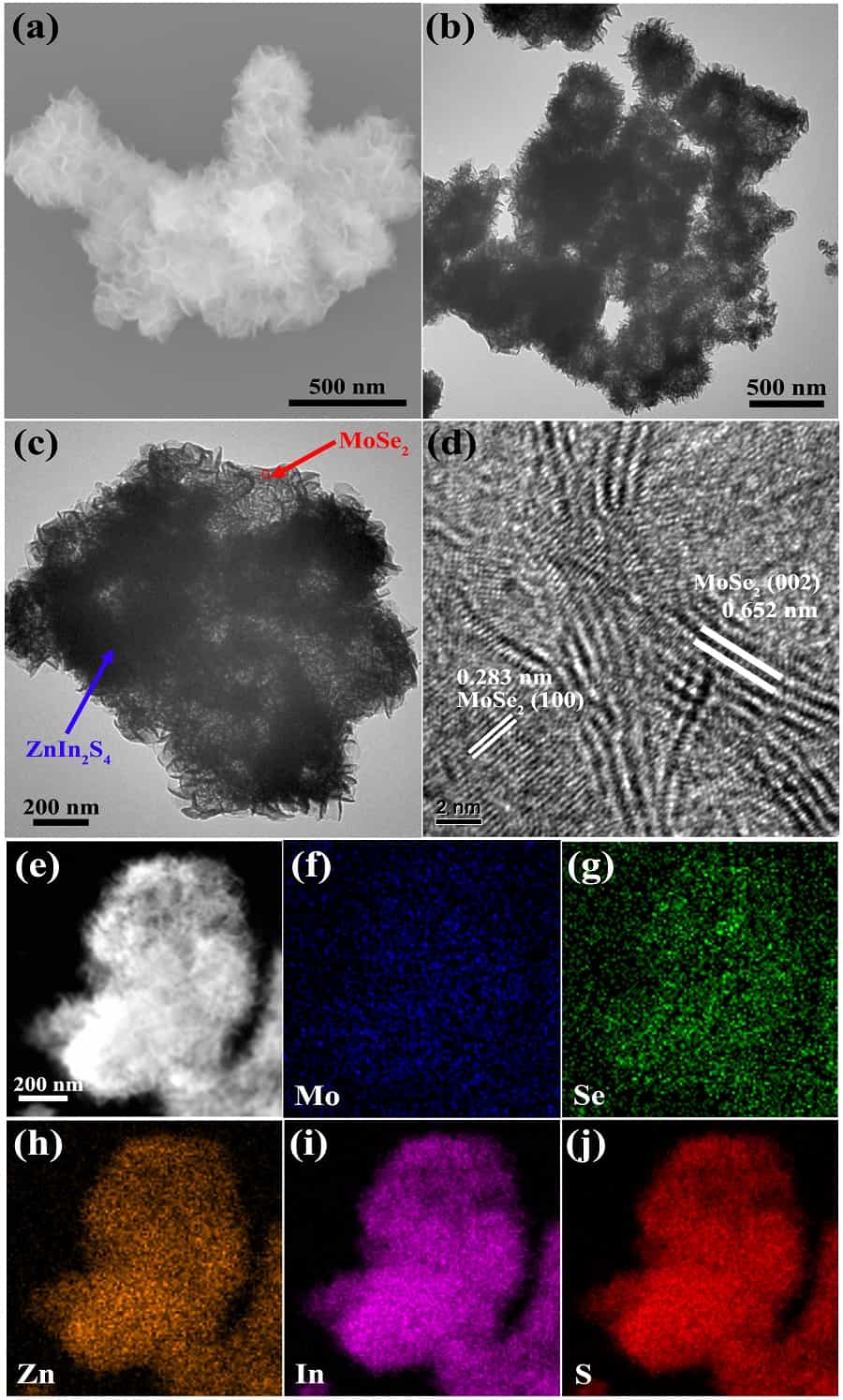
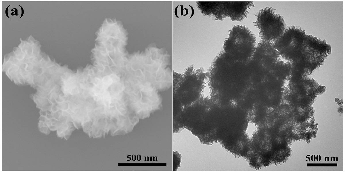
To elucidate the role of nanostructures in producing a highly efficient photocatalyst, a range of state-of-the-art techniques such as X-ray diffraction, electron microscopy and energy-dispersive X-ray (EDX) mapping were employed. EDX is an incredibly useful spectroscopic tool that enables elemental analysis down to the nanometre length scale, and in this instance it shows the coexistence of Zn, In, S, Mo and Se in the hybrid system (see image). Further morphological insights from the remaining characterization techniques delve into how the structure gives rise to high chemical reactivity.

Ong explains that “importantly, the MoSe2 nanonetworks have multiple pores and are in favour of the direct light absorption of ZnIn2S4, even though the ZnIn2S4 is hybridized with MoSe2. The ZnIn2S4/2%MoSe2 photocatalyst displays a dramatically high noble-metal-free hydrogen generation rate of 2228 μ mol g–1 h<sup–1 sup=””>with a high apparent quantum yield of 21.39% at 420 nm.”</sup–1>

This system signifies a massive enhancement in the production of hydrogen, weighing in at more than two times larger than similar systems. The apparent quantum yield is a measure of how many reactive electrons are produced depending on the amount of incident light (at a 420 nm wavelength in this instance, which corresponds to violet light); in the world of photocatalysis, 21% is a very impressive figure.

To the future and beyond

To fully investigate the mechanisms and applications of this material, various photoelectrochemical tests were carried out, with promising performances, demonstrating that this system can be used as a basis for future commercialization. However, the work does not stop there, and as Ong reveals to nanotechweb.org, “besides water splitting, my research direction is now gearing toward diverse types of energy conversion, including photocatalytic, photothermal, photoelectrochemical and electrochemical CO2 reduction and N2 fixation.” So watch this space for even more future energy solutions.

Full details of the research are reported in ChemSusChem DOI: 10.1002/cssc.201701345, published as a contribution to the Special Issue “Artificial Photosynthesis for Sustainable Fuels” invited by the editor-in-chief.

Muons reveal hidden void in Egyptian pyramid

A large void hidden deep within Khufu’s Pyramid at Giza in Egypt has been discovered by a team of physicists. The first-ever image of the mysterious structure was taken using muons that shower down on Earth after being created when cosmic rays collide with the atmosphere.

The measurements were done by the ScanPyramids collaboration that includes researchers from Egypt, Japan and France. The team used three different muon-imaging techniques to study the pyramid, which was built in about 2500 BCE and is also known as the Great Pyramid and the Pyramid of Cheops.

Unexpected muons

Called muography, the technique is similar to radiography using X-rays. Dense materials such as stone tend to absorb muons, which travel relatively unhindered through the air. If more muons than expected reach a detector within the pyramid, it means that they must have passed through an air-filled void on their way.

In 2016 chemical-emulsion muon detectors developed at Nagoya University in Japan were deployed in the Queen’s Chamber, which is the lowest known chamber within the pyramid (see figure). Much like photographic film, the emulsion undergoes a chemical reaction when exposed to muons. This leaves permanent 3D tracks in the detector that tell the researchers the directions from which the particles came.

As well as detecting known voids such as the King’s Chamber, the emulsion detectors provided the first evidence for a previously-unknown large void about 30 m in length. “We knew we had found something very big and important,” says Mehdi Tayoubi of the Heritage Innovation Preservation Institute and Dassault Systèmes – both in Paris.

To verify the existence of the void, scientists from the KEK particle physics lab in Japan installed hodoscopes at a separate location within the Queen’s Chamber. These comprise layers of plastic scintillator, which measure muon trajectories. Outside the pyramid, physicists from France’s nuclear research agency CEA monitored the muon flux through the pyramid using micromegas detectors. These were arranged in muon “telescopes”, which are also able to measure muon trajectories.

We knew we had found something very big and important
Mehdi Tayoubi, Heritage Innovation Preservation Institute

Computer reconstruction

Using what are essentially three different 2D images taken from three different angles, the team could locate the void in 3D. A computer reconstruction based on analysis of the data suggests that it is similar to the Grand Gallery of the pyramid – which is an inclined passageway about 2 m wide, 8 m high and about 47 m long. The new void is between 50 and 70 m above ground level, which puts it above the Grand Gallery. The void is at about the same level as a series chambers that are above the King’s Chamber – which lies near the centre of the pyramid. Tayoubi says that it is not clear whether the void is a single chamber or multiple chambers, or whether it is horizontal or inclined.

“The void is not predicted by any theory about the pyramid,” says Tayoubi. He hopes that experts in ancient Egyptian architecture will be able to provide further information that could then be combined with the muon data in computer simulations in to determine what the void could be.

Very difficult to reach

He says that the location of the void would make it very difficult to reach by drilling and adds: “Our mission is non-destructive by design.” However, he points out that the Nagoya team has also found a corridor-like structure near the surface of the pyramid that could provide a route to the newly discovered void.

This is not the first time that muons have been used to study the interior of pyramids. In the 1960s the American physicist and future Nobel laureate, Luis Alvarez, placed a muon detector in a chamber in the nearby Pyramid of Khafre. He showed that there are no other large chambers in that pyramid.

More recently, Arturo Menchaca of the National Autonomous University of Mexico placed a detector inside the Pyramid of the Sun at Teotihuacan near Mexico City. Physics World‘s James Dacey and Matin Durrani visited the experiment in 2015, where they recorded the podcast “Inside the particle pyramid“. Dacey recounts how the intrepid pair crawled into the interior of the pyramid in “Particle-physics lab beneath a Mexican pyramid“.

Elsewhere in Mexico, a team including Menchaca is trying to image the interior of a volcano using muons. See “Monitoring a smoking giant“.

Under the sea

In the deep, dark depths of the ocean, where chimneys spout hot black clouds of particles, there is life. Scientists are currently exploring the sea floor of the eastern Pacific Ocean using the research ship Nautilus, aided by its two hardy assistants Argus and Hercules – remotely operated vehicles. Gaining a better understanding of these harsh environments offers clues about whether life could survive on other worlds, and could inform future missions to Jupiter’s watery moon Europa. This video introduces the aims and the technology of the Nautilus mission, including video footage of the alien landscape that lies beneath the waves.

Find out more about the Nautilus mission in November’s Physics World, a special issue about the challenges for physicists working below the waterline. The issue includes an article by astronomer and science communicator Jon Willis about his time spent on the Nautilus ship earlier this year. Physics World managing editor Matin Durrani introduces our “Under the sea” special issue and explains how you can access it in this article published yesterday.

Nanoflowers harness sunlight

Nanoarchitectures reveal the inner workings of a new breed of photocatalysts

Finding ways to effectively utilise the vast quantities of sunlight that impart energy to our planet remains the greatest challenge for many alternate energy visionaries. Among them is Wee-Jun Ong who is at the forefront of research into photocatalysis. As part of a publication showcasing promising new  methods for solar energy conversion, Ong  has stated that accomplishing solar-to-energy conversion will, in turn, lead to the development of a sustainable, green, and renewable future without environmental detriment. All of us need to do our roles to make this world better.”

Reporting in ChemSusChem Ong and colleagues show that submicron flower-like structures created by a one-pot production method have high photocatalytic activity, specifically for water splitting to produce hydrogen. The work, a collaboration between Singaporean and Chinese institutions, represents the forefront of visible light-driven hydrogen evolution research that is both effective and environmental. The nanostructures do not contain precious metals and so could provide a path toward cost-effective and environmentally friendly energy conversion.

In combining both sunlight and water to create hydrogen, lead author Deqian Zeng and colleagues including Ong make use of naturally abundant resources, a factor that is key in providing a sustainable future for us all. This hydrogen can be used as a clean fuel source, but arguably more important is the alluring potential that has been unearthed in using hierarchical nanostructures for potential application to a wide variety of energy storage and conversion applications.

Less precious, more efficient

Zeng et al. present an attractive alternative to current water-splitting processes, which rely heavily on precious metals. The use of precious, or noble, metals is not ideal as the metals are just that: precious as they are in limited supply, and therefore expensive both in terms of monetary cost and the environmental impact in mining them. By combining ZnIn2S4 and MoSe2 heterostructures, the researchers have developed novel photocatalysts from abundant materials with highly desirable properties including non-toxicity, high chemical stability and superb catalytic activity.

The properties are particularly impressive considering that the production method is much quicker and much simpler than competing processes: a reaction duration of just one hour makes use of a solution-phase hybridization approach that needs only a single pot to fabricate. This is a marked improvement compared with alternate methods that traditionally involve complex, multi-step reactions over the course of days.

Nanoflowers for photocatalysis

Wee-Jun Ong, corresponding author for this research

To elucidate the role of nanostructures in producing a highly efficient photocatalyst, a range of state-of-the-art techniques such as X-ray diffraction, electron microscopy and energy-dispersive X-ray (EDX) mapping were employed. EDX is an incredibly useful spectroscopic tool that enables elemental analysis down to the nanometre length scale, and in this instance it shows the coexistence of Zn, In, S, Mo and Se in the hybrid system (see image attached to article). Further morphological insights from the remaining characterisation techniques delve into how the structure gives rise to high chemical reactivity.

Ong explains that importantly, the MoSe2 nanonetworks have multiple pores and are in favour of the direct light absorption of ZnIn2S4, even though the ZnIn2S4 is hybridised with MoSe2. The ZnIn2S4/2%MoSe2 photocatalyst displays a dramatically high noble-metal-free hydrogen generation rate of 2228.

This system signifies a massive enhancement in the production of hydrogen, weighing in at over two times larger than similar systems. The apparent quantum yield is a measure of how many reactive electrons are produced depending on the amount of incident light (at a 420 nm wavelength in this instance, which corresponds to violet light); in the world of photocatalysis, 21% is a very impressive figure.

To the future and beyond

To fully investigate the mechanisms and applications of this material, various photoelectrochemical tests were carried out, with promising performances demonstrating that this system can be used as a basis for future commercialisation. However, the work does not stop there, and as Ong reveals to Physics World, “besides water splitting, my research direction is now gearing toward diverse types of energy conversion, including photocatalytic, photothermal, photoelectrochemical and electrochemical CO2 reduction and N2 fixation.” So watch this space for even more future energy solutions.

Full details of the research are reported in ChemSusChem, published as an invited contribution to a Special Issue of the journal ChemSusChem, Artificial Photosynthesis for Sustainable Fuels by the Editor-In-Chief. DOI: 10.1002/cssc.201701345

Copyright © 2026 by IOP Publishing Ltd and individual contributors