Like a two-lane highway with one lane empty and the other clogged with traffic, superconducting diodes allow electrons to flow without resistance in one direction while encountering normal, resistive conditions in the other. First demonstrated experimentally in 2020, these devices have considerable potential as platforms for fundamental studies of quantum materials and as building blocks for superconducting electronics.
For many applications, being able to control the flow of electricity through the diode – or even reverse its polarity – is essential. In principle, there are several ways of doing this because the efficiency of the superconducting diode effect (SDE) depends on many factors. Examples include magnetic field, temperature and diode design as well as intrinsic properties such as the momentum of the Cooper-paired superconducting electrons and their spin-orbit coupling.
In practice, though, some of these properties are more easily changed than others. To return to the highway analogy, it’s much more straightforward to alter the flow of traffic by posting new road signs, rather than by rebuilding the road or redesigning the cars.
In a recent paper in Chinese Physics Letters, Yanwu Xie, Yishuai Wang, Wenze Pan and Meng Zhang of Zhejiang University in Hangzhou, China describe a new superconducting diode platform that makes it far easier to change the device’s configuration, and thus to control the flow of superconducting electrons through it. Physics World spoke to them about their research and its possible applications.
How did you get the idea for this new type of superconducting diode?
This work started with an unexpected experimental observation. While we were making routine current-voltage measurements on a conventional strip-shaped superconducting device constructed at the interface between two materials, LaAlO3 and KTaO3 (LAO/KTO), we noticed a pronounced difference between the critical currents in opposite directions. Given the growing interest in the SDE, this surprising result immediately caught our attention and prompted us to investigate its origin.
What is special about these two materials?
The properties of conventional superconducting diodes are typically locked into their fixed physical structures, such as Josephson junctions or patterned vortex pinning sites. This inflexibility makes post-fabrication tuning or reconfiguration of the diode characteristics extremely challenging.
Two-dimensional oxide interface superconductors such as LAO/KTO and LaAlO3/SrTiO3 are good candidates for overcoming this problem. The strong spin-orbit coupling near the interface enables possible finite-momentum Cooper pairing, while the extremely low superfluid density and intrinsic two-dimensional nature of the materials create ideal conditions for studying vortex dynamics and magnetic flux behaviour.
In addition, these systems have exceptional tuneability. Their superconducting states can be well controlled through both global substrate gating and local conductive atomic force microscope (cAFM) lithography, which opens new possibilities for post-fabrication SDE engineering.
What was the most challenging aspect of this research?
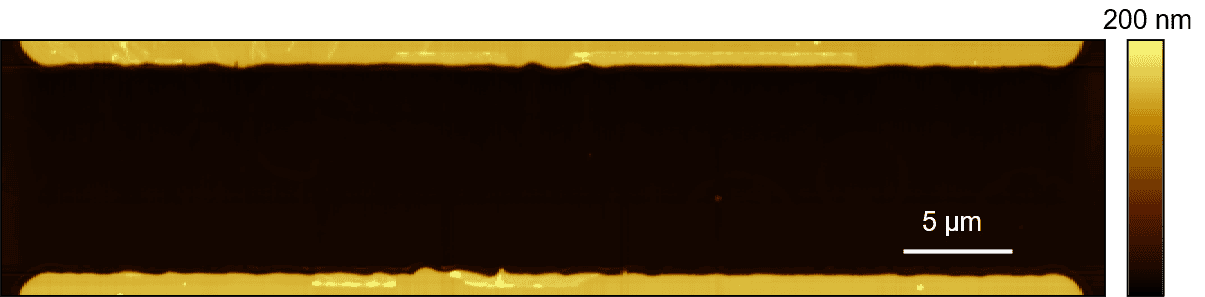
The most challenging part was unravelling the frustrating sample-to-sample variability we encountered early on. We now know that the SDE in conventional LAO/KTO devices stems from asymmetric vortex entry conditions caused by random, fabrication-induced edge imperfections. At the time, however, even devices with nominally identical geometries exhibited wildly different SDE efficiencies and polarities, showing no discernible systematic trend.
The breakthrough came when AFM imaging revealed random edge defects on the superconducting channels. To test whether these random imperfections were indeed the root cause, we used cAFM lithography to “straighten” the originally photolithography-produced rough channel boundaries. This atomic-scale trimming strongly suppressed the SDE, providing unambiguous evidence for the vortex edge asymmetry mechanism.
We then turned this challenge into an opportunity. By using cAFM to re-shape the channel edges repeatedly and in a non-volatile way, we transformed a source of random sample variability into a tool for deterministic, on-demand quantum device control.
What are some possible applications for this editable superconducting diode?
The nonreciprocal transport of charge carriers – exemplified by p-n junctions in semiconductor diodes – is a cornerstone of modern electronics. Similarly, superconducting diodes are emerging as pivotal components for superconducting electronics. What distinguishes our approach is our ability to reversibly modify the diode polarity and efficiency within the same device through nanoscale control of the superconducting channel geometry. This editability may enable reconfigurable superconducting circuit elements and adaptive circuit architectures, while also providing a versatile platform for investigating the role of geometry-associated vortex dynamics in nonreciprocal superconducting transport.
What will you do next?
We plan to fully exploit the unique cAFM lithography capability of our oxide interface platform to systematically investigate how tailored vortex-boundary configurations shape the SDE. The diode performance can be further optimized by mapping out the precise relationship between channel geometry, vortex entry barriers and rectification efficiency.
Scientists unveil Josephson diode

In parallel, we plan to introduce artificial pinning centres (such as nanoscale insulating dot arrays) directly into the superconducting channel. This will allow us to engineer asymmetric vortex-pinning landscapes within the bulk of the channel. Combining this engineered flux pinning with the asymmetric vortex-boundary mechanism demonstrated in the current work offers a promising route toward achieving a robust, deterministic and highly controllable superconducting diode.