The remarkable properties of carbon nanotubes may allow them to play a crucial role in the relentless drive towards miniaturization at the nanometre scale
Nanotechnology is predicted to spark a series of industrial revolutions in the next two decades that will transform our lives to a far greater extent than silicon microelectronics did in the 20th century. Carbon nanotubes could play a pivotal role in this upcoming revolution if their remarkable electrical and mechanical properties can be exploited.
Since the first measurements were made in 1997, these rolled up sheets of graphite have captured the imagination of researchers around the world. Progress in understanding the basic physics and chemistry of nanotubes has advanced at a phenomenal rate – and shows no signs of slowing.
Nanotubes have an impressive list of attributes. They can behave like metals or semiconductors, can conduct electricity better than copper, can transmit heat better than diamond, and they rank among the strongest materials known – not bad for structures that are just a few nanometres across. Several decades from now we may see integrated circuits with components and wires made from nanotubes, and maybe even buildings that can snap back into shape after an earthquake.
Nanotubes as test tubes
Carbon nanotubes were first observed in 1991 by Sumio Iijima at NEC in Japan. These so-called multiwall nanotubes consisted of several concentric tubes of carbon nested inside each other. Two years later Iijima, Donald Bethune at IBM in the US and others observed single-wall nanotubes just 1-2 nm in diameter. But the field really took off a few years later when various groups found ways to mass-produce high-quality nanotubes.
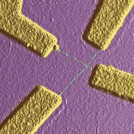
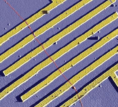
Paul McEuen describes how the remarkable electrical properties of single-wall nanotubes stem from the unusual electronic structure of graphite. A nanotube can be either a metal or a semiconductor depending on the way the graphite sheet is rolled up. Metallic nanotubes are also ideal systems in which to explore electron transport in one dimension thanks to their near-perfect structures.
Other fundamental phenomena in quantum physics can be tested on multiwall nanotubes, as Christian Schönenberger and Lazslo Forró explain. Researchers expect to find more complex behaviour for multiwall nanotubes due to the interactions between adjacent layers.
Applications and challenges
Industry has begun to notice the unique properties of carbon nanotubes, as Walt de Heer and Richard Martel report. The first commercial device that uses multiwall nanotubes may be a lamp that operates on the field-emission principle. Moreover, the field-emitting characteristics of carbon-nanotube films have attracted serious interest from the giants of the display industry. Samsung, for example, plans to market a flat-panel colour display made from multiwall nanotubes within two years. Meanwhile, research at IBM indicates that nanotubes transistors should be competitive with state-of-the-art silicon devices. Nanotubes could also be used to store hydrogen to power electric vehicles.
However, many technological hurdles need to be overcome before large-scale applications reach the marketplace. For example, the techniques that are used to build electronic components from nanotubes are painstaking and utterly inappropriate for mass production. But perhaps the most severe limitation is that high-quality nanotubes can only be produced in very limited quantities – commercial nanotube soot costs 10 times as much as gold!

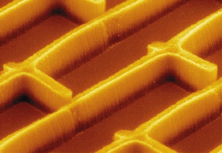
Hongjie Dai describes how researchers are learning to control the growth of carbon nanotubes, and manufacture them more efficiently. These techniques have produced ordered nanostructures with advanced properties.
Although there are many challenges ahead, nanotubes appear destined to open up a host of new practical applications and improve our understanding of basic physics at the nanometre scale.