One of the main challenges in developing "photonic crystals" - materials which have photonic band gaps in much the same way that semiconductors have electronic band gaps - is to make structures which operate at visible wavelengths. Photonic crystals are made by drilling holes in a material. The dimensions and spacing of the holes determine the wavelength at which the crystal operates. Now Andrew Turberfield and colleagues at Oxford University in the UK have developed a new technique for making photonic crystals for visible radiation that could lead to a new generation of photonic integrated circuits (Nature 404 53).
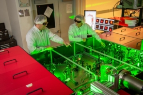
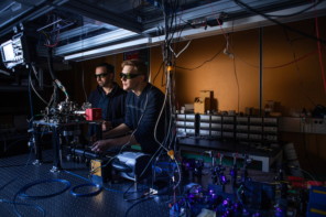
The method works by solidifying a resin that hardens when exposed to light. The resin is solidified into a three-dimensional grid by placing it in the interference pattern set up by four intersecting laser beams. The pores in the resin are then filled with titanium dioxide, which is allowed to set. The resin is then burnt off to create the photonic crystal.
Other techniques for making photonic crystals rely on chemical deposition, or on adapting semiconductor fabrication techniques. However, both of these methods have a number of disadvantages. “Our technique is much more flexible than other methods,” says Turberfield. “It is fast, cheap, and very flexible.” The technique can also create structures with 10 times as many layers as structures produced by chemical deposition.
The next step, says Turberfield, is to create a material that has the same optical characteristics in all directions, and then introduce defects into the crystal. This will allow a wide range of photonic-based circuits to be fabricated.


