Silicon chips could be made more quickly and cheaply using a new technique developed by physicists in the US. Stephen Chou and colleagues at Princeton University have successfully imprinted patterns onto silicon using quartz moulds instead of the usual combination of lithography and etching. With a resolution of just 10 nm and an ‘imprint time’ of 250 ns, the new process could revolutionize the semiconductor industry – and keep ‘Moore’s Law’ on track for another 25 years (S Chou et al 2002 Nature 417 835).

The components on a microchip are made by carving patterns into layers of doped and undoped silicon. In the standard technique, light is shone through a stencil onto a silicon wafer that is coated with a light-sensitive polymer known as a resist. Chemical etching then removes the regions of silicon coated with either the unexposed or the exposed polymer, until the desired structure is achieved. Finally, the remaining polymer is washed off.
But such ‘photolithography’ is expensive and complex, and the resolution of the technique is fast approaching the diffraction limit. This means that it will not be able to make features much smaller than the current minimum size of about 130 nm – and that the semiconductor industry could soon violate one of its guiding principles, known as Moore’s Law. Coined in 1965, this law described how the density of components on a chip doubled every 18 months, and was soon adopted by the semiconductor industry as a target.
Now Moore’s Law could be back on track. Chou and co-workers say that their technique – known as laser-assisted direct imprint – can create features as small as 10 nm on silicon wafers. The new process also eliminates the need for the resist and washing steps.
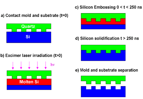
The team inscribed the pattern into a quartz mould using ‘impact lithography’, which is much cheaper and easier than the photolithography of silicon. The mould was then placed on top of a silicon wafer. A pulse of light from a helium-neon laser – with a wavelength of 633 nm – was then fired through the mould to melt the top layer of silicon. The researchers then pressed the mould into this liquid silicon and removed it after the silicon had solidified, leaving the pattern.
Since silicon reflects more light as a liquid than it does as a solid, the team could tell when the mould needed to be removed by measuring how much of the laser pulse was reflected. The researchers also say that the mould can be used several times.
The Princeton team now hopes that its technique will be taken up by the semiconductor industry. “A prototype machine could be available in three years,” Chou told PhysicsWeb. The team also believes it should work on silicon wafers up to eight inches in diameter, and could be adapted for other materials and processes. “There are some technical issues in scaling up, but there are no fundamental issues,” he says.


