Researchers at Hewlett-Packard claim to have created the highest density electronically addressable memory to date. The 64-bit memory uses molecular switches and has an area of less than one square micron. The device has a bit density that is more than 10 times that of current silicon memory chips.
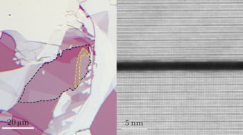
The researchers made the device by creating a master mould of eight 40-nm wide parallel lines, which pressed into a polymer layer on a silicon wafer to make eight parallel trenches. After filling these trenches with platinum to form wires, the scientists deposited a single layer of electronically switchable molecules onto the surface. Finally, they rotated the mould and made another eight wires that ran perpendicular to the first set on top of the molecular layer.
The resulting device contained 64 regions where the top and bottom wires crossed. A bit of memory sat at each of these points, with roughly 1000 molecules sandwiched between the upper and lower wires. To write a bit, the researchers applied a voltage pulse to set the molecules’ electrical resistance. Measuring the molecules’ resistance at a lower voltage, meanwhile, allowed them to read the bit.
“We believe that molecular electronics will push advances in future computer technology far beyond the limits of silicon,” said R Stanley Williams, director of Quantum Science Research at HP Labs. “Capacity and performance could be extended enormously by layering molecular-switch devices on conventional silicon without the need for complex and expensive changes to the base technology.”
The team used acombination of optical and electron-beam lithography and say that it took about a day to create the master, which included 625 separate memories connected to conventional wires so that they could communicate with them. “After that, it took just a few minutes to make an imprint,” said Williams.
The researchers also put logic in the same circuit by configuring molecular-switch junctions to make a demultiplexer – a logic circuit that uses a small number of wires to address memory. HP Labs says that demultiplexers are essential to make memories practical.
“This is the first demonstration that molecular logic and memory can work together on the same nanoscale circuits,” added Williams. The memories are also rewritable and non-volatile, that is, unlike today’s DRAM (dynamic random access memory) chips, they preserve information stored in them after the voltage is removed.
Williams made the announcement last week at a symposium celebrating the 175th anniversary of the KTH Royal Institute of Technology in Stockholm, Sweden. HP Labs has received four US patents in connection with the work.