Physicists at Cambridge University in the UK and the Japan Science & Technology Corporation in Tokyo have exploited a “natural” system of tunnel barriers in nanocrystalline silicon to make a single-electron transistor that operates at room temperature. The researchers say that the technique used to fabricate the transistor is compatible with existing silicon technology and has “considerable processing advantages” over the techniques previously used to make similar devices (Y T Tan et al. 2003 J. Appl. Phys. 94 633).

A single-electron transistor consists of a conducting ‘island’ that is separated from the source and drain terminals by tunnel barriers (see figure). Electrons can only transfer between the island and the source and drain terminals by quantum tunnelling through the barriers. For such devices to operate at room temperature, which is essential if they are to be used in realistic circuits, the islands must be smaller than 10 nanometres across. Moreover, the potential energy of the tunnel barriers must be high enough to localize electrons on the island.
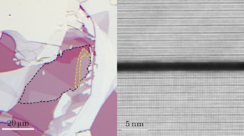
In 2001 the Cambridge-Tokyo team made single-electron transistors from thin films that contained nanocrystalline silicon grains that were embedded in an amorphous silicon matrix. “In such material, the grains ‘naturally’ form the islands required by a single-electron transistor and the grain boundaries ‘naturally’ form the tunnel barriers needed to confine the electrons on the grains,” team member Zahid Durrani told PhysicsWeb. While that single-electron transistor worked at 60 Kelvin, the potential energy of the tunnel barriers was only 40 meV, which was too low for the device to work at higher temperatures.
The team has now increased this energy to 173 meV, which means that the transistor is able to operate at 300 K. “We use low-temperature oxidation to oxidise the grain boundaries from amorphous silicon into silicon dioxide,” said Durrani. “This wraps each grain in silicon oxide and allows us to increase our tunnel barrier height so that electrons can be confined on the grains at room temperature.”