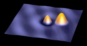
Researchers at IBM Zurich Research Laboratory, Switzerland, and Chalmers/Göteborg University in Sweden have used a scanning tunnelling microscope (STM) to add and remove single electrons from individual gold adatoms. The technique could ultimately lead to memory devices that store each bit on just one atom ( J Repp et al. 2004 Science 305 493).

“In 1990, Don Eigler of IBM’s Almaden Research Center showed that, using an STM, atoms can be placed on top of a surface with atomic precision,” says Jascha Repp of IBM. “Now the next step has been achieved by manipulating the charge state of an atom without moving it to another adsorption site and without changing its chemical surrounding.”
Repp and colleagues used a home-built STM with an electrochemically etched tungsten wire as the tip, operating the kit at temperatures between 5 and 60 kelvin. They adsorbed gold atoms onto an insulating film of sodium chloride just two or three atomic layers thick on top of a copper single-crystal. The adatoms positioned themselves on top of the Cl– ions.
To alter the charge state of a gold adatom, the researchers simply applied a voltage pulse to it using the STM tip. Applying a voltage of +0.6 volts for a few seconds caused the tunnelling current to drop by about a third. The image of the adatom also took on a sombrero-like shape, with a protrusion about 0.5 Angstrom less high than before and a trough appearing around it. Applying a negative voltage of about -1 volts returned the adatom to its original state.
The experiments indicated that the original gold adatoms were in a neutral state while applying a positive voltage gave the adatoms a negative charge. “The chemical and physical properties of ions in general are qualitatively different from those of the corresponding neutral atoms,” said Repp. “Therefore our findings will have an impact not only on physics, but also on chemistry.”
Repp says that the controlled deposition and removal of an electron charge onto and from an individual atom is a decisive step towards future atomically small devices. “For instance, it could lead to a non-volatile memory cell at the ultimate spatial limit, where one bit of information is stored on a single atom,” he explained. “Practical atomic-scale memories would increase the amount of data that can be stored on a given area by at least ten thousand times.”
The technique could perhaps also tailor material properties at the atomic level. “The switching between different charge states of an individual atom enables the control of, for example, chemical reactivity, optical properties, or magnetic moment,” said Repp. “Owing to the long-range nature of electrostatic forces, even the properties of molecules may be controlled through the change in charge state of an atom nearby.”
The aim of the Swiss-Swedish researchers is to study electron current through man-made atomic structures that are electronically decoupled from a metal substrate and perfectly arranged down to the atomic-length scale. “To reach this goal we study the controlled lateral positioning of atoms as well as larger molecules on ultra-thin insulating films,” said Repp. “We want to use the control of the charge state of individual atoms to influence the assembly of such atomic-scale structures and also to switch or guide the electron current through them.”


