Physicists in Ireland have developed a novel technique that allows "hands-free" manipulation of mesoscale device components for the first time. The method employs electric fields to direct the assembly of the components into integrated systems and could be an alternative to conventional techniques for making electronic devices (A O'Riordan et al. 2004 Nano Letters 4 761).

Mesoscale components have dimensions that lie between those of individual molecules, which are nanometres across, and millimetre-sized macroscopic objects. Light emitting diodes and other systems that contain mesoscale components are assembled by micro-robotic “tweezers” that pick up individual devices and place them on pre-selected positions on a chip surface. A typical commercial optoelectronic assembly machine, for instance, can make up to 250 devices per hour and can pick-and-place devices with dimensions of around 250 microns by 300 microns.
However, as devices continue to decrease in size, manipulating them in this way will become more difficult. This is because adhesive forces — electrostatic, van der Waals and capillary forces — between the device and the tweezers will begin to dominate the gravitational forces needed to release the device.
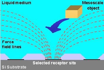
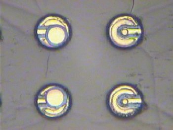
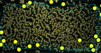
The method developed by Alan O’Riordan and colleagues at the National Microelectronics Research Centre (NMRC) in Cork exploits the fact that most devices are charged and therefore respond to an appropriately configured electric field. This field can be used to direct and accurately position a device on a chip substrate, eliminating the use of tweezers altogether (see figure 1). To test their technique, the team assembled a semiconductor-based light emitting diode on a silicon chip (see figure 2 for a video of the process).
“Field configured assembly (FCA) is an integration technology inspired by self-assembly processes in nature,” O’Riordan told PhysicsWeb. “However, it is compatible with contemporary optoelectronic manufacturing methods and permits low cost, rapid and scalable assembly and integration of devices.”


