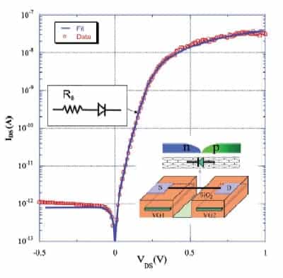
A physicist has made the best ever p-n junction diode from a carbon nanotube. The current-voltage characteristics of the device exhibit an "ideality factor" of one, which is the maximum possible value for any diode. The new diode could have applications in electronics, sensors and photovoltaics (Appl. Phys. Lett. 87 073101).

The feature sizes in conventional microelectronic circuits are getting smaller and smaller and look set to reach the limit imposed by the fundamental properties of silicon in a decade or so. The semiconducting properties of carbon nanotubes – rolled up sheets of graphite just nanometres in diameter – make them a promising alternative to silicon, and nanotubes have already been used to fabricate a variety of electronic components, including diodes and field-effect transistors.
Diodes are fundamental semiconductor devices that form the basic building blocks of many electronic devices, such as transistors and light-emitting diodes (LEDs). A diode is normally made by joining a p-type semiconducting material — which has been doped with impurities to add extra “holes” — to an n-type semiconductor that has an excess of electrons. However, it is almost impossible to do this in a carbon nanotube.
Last year, Ji Ung Lee of GE Global Research in New York solved this problem by using an electric field to create the p and n regions instead. He placed two separate gates underneath a single-walled nanotube so that one gate coupled to one half of the nanotube and the other gated coupled to the other half. By biasing one gate with a negative voltage and the other with a positive voltage, he created a p-n junction that behaved as an almost ideal diode.
Lee made his device using standard optical lithography techniques and placed the carbon nanotube on top of a silicon dioxide substrate, which acted as the gate dielectric. Now, he has transformed this structure into an ideal diode by simply suspending the nanotube across two silicon dioxide slabs (see figure). According to Lee, the nanotube no longer interacts with the surface on which it rests which means that extra states that can lower the device’s performance are not created. It may also be possible to make the diode operate as an LED.
“My results are not only a direct confirmation of the structural purity of single-walled nanotubes but a strong affirmation of their potential as electronic materials,” says Lee. He now plans to further investigate the optical properties of the nanotubes and make a photodetector.


