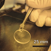
Imagine solar cells that are flexible enough to be rolled up like a sheet of paper or so transparent that they can be hung over a window. Such solar cells are a step closer now that researchers in the US have devised a new method for printing thin wafers of silicon onto many other types of material.
John Rogers and colleagues at the University of Illinois at Urbana-Champaign and Northwestern University liken their method to the way a rubber stamp transfers ink from a pad to paper. First, they etch a striped pattern onto a wafer of crystalline-silicon (the “pad”) before lifting the resulting segments (the “ink”) with a soft piece of polymer (the “stamp”). Then they push the polymer onto the desired substrate (the “paper”) to print on the segments. Finally they evaporate metal onto the back of the material and etch it to leave electrodes running down the sides (Nature Materials advance online publication doi:10.1038/nmat2287).
The benefit of this stamp method is that Rogers and colleagues can use a wide variety of substrate materials, including flexible plastics. Although other researchers have tried to make flexible cells before — for example, using amorphous silicon or polymers for the active material — the performance or reliability of the cells has always suffered. In tests, Rogers and colleagues’ cells had a solar-energy conversion efficiency of 7.2% — significantly under commercial devices, which operate at about 18% — though were flexible enough to be rolled around a pencil.
Another advantage of the US team’s method is that the cells can be printed thinly or in sparse arrays so that they are partially transparent, which means they could, for example, be fixed over windows. Using sparse arrays, Rogers and colleagues could vary the transparency between 35 and 70%.
Rogers told physicsworld.com that his team has created a start-up company called Semprius Inc to develop commercial devices, although it will be focusing on gallium arsenide (GaAs) — a more expensive though more efficient material than silicon — for the cell designs. “GaAs appears to offer the greatest near-term commercial potential,” he says.
Aside from working on GaAs themselves, Rogers’s team is now exploring the different cell layouts so that they can get high efficiencies while still using cheaper, low-purity silicon. “This important capability, which is suggested by our theoretical modelling efforts, could reduce substantially the cost of the silicon,” he adds.