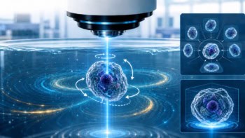
Researchers in the US are the first to use electric fields to guide DNA-coated nanowires to specific locations on a chip. The technique, which allows the nanowires to be attached directly to chip circuitry, could come in handy for making a variety of nanoscale devices, such as medical biosensors that detect cancer or harmful bacteria and viruses. It also offers a way to incorporate new types of components within conventional silicon electronics.
Theresa Mayer and Christine Keating of Penn State University and colleagues were able to control exactly where nanowires were placed on different, predetermined locations on a chip with sub-micrometre accuracy, and then make individual contacts to each wire without losing or inactivating the DNA that was on the wires (Science 323 352). Placing the nanowires accurately in this way is crucial for making individual contacts between nanowires and other devices on a chip such as a transistor.
Mayer and Keating’s technique involves generating electric fields at desired locations on the chip by applying alternating voltages between pairs of guided electrodes patterned on the chip surface. The nanowires are drawn into the regions of highest electric field strength, which are found in the wells between the guiding electrodes. The researchers place a second set of wires into the next set of microwells by applying voltages to a new pair of guiding electrodes, and so on. Combining electrodes and wells in this way results in sub-micrometre positioning control, they say.
Variety of configurations
In the experiment, the different tagged nanowires were placed in rows but they could be positioned in a variety of configurations.
The nanowires are coated with DNA in separate batches before they are assembled onto the chip. Different wires, that is those carrying different sequences of DNA, are assembled into the selected wells. The sample is then exposed to a suspension of the next type of wires, which have a different DNA sequence on them.
“We control where the different types of wires go by where we apply the alternating voltage,” Mayer told physicsworld.com.

The scientists say that the technique is fairly simple and could be scaled-up for industrial manufacture. According to the team, the most obvious application for the technique is in on-chip, electronic biosensors that could ultimately lead to portable, low-power detectors for pathogens and diseases like cancers.
Avoiding false negatives
“Having many copies of each type of nanowire in the array would help avoid false negatives and positives, and enable screening for multiple target sequences at once,” explained Keating.
Biosensors would not be the only beneficiaries: being able to control the location of device components prepared off-chip also offers a route to incorporating non-traditional device components with conventional silicon electronics, say the researchers.
Keating adds that she ultimately envisions multi-analyte biosensors in which binding events are detected as electrical responses by thousands or even millions of individual nanowires and are processed by electronic circuits directly on the chip. In the present work, the team was able to show assembly of many copies of each of three different DNA-coated wire populations. So far, they have used fluorescence to follow DNA binding but plan to perform on-chip electrical detection soon.
“We are also very interested in exploring what other types of materials and coatings can be assembled and integrated with the on-chip electronics using our technique,” said Keating. “We believe this could be a very general approach to incorporating new materials that are difficult or impossible to prepare in place on a chip.”