Researchers at the University of Maryland in the US are the first to have observed an insulating state at the surface of bismuth selenide. This material is normally a strong “topological insulator”, which means that it is insulating in the bulk but conducting at the surface. The new finding could lead to applications in spintronics and even quantum-information technologies.
The conducting surface in bismuth selenide (Bi2Se3) arises from the topology of the material’s band structure and means that the electrons on the surface cannot be localized – that is, cannot become insulating. “A number of interesting properties are associated with this topological surface state,” explains team leader Michael Fuhrer. “These include the fact the surface state is completely spin polarized and any charge current present will necessarily carry a spin current.”
However, researchers have predicted that the conducting surfaces on the top and bottom surfaces of a Bi2Se3 slab should be able to couple if brought close enough together and that such contact should lead to an insulating state. “This is what we have now observed in our experiments,” says Fuhrer, “that very thin [3 nm] Bi2Se3 crystals are in fact conventional insulators.”
Confining electrons
The result is important because it means that electrons can be confined in the surface state of the material by creating insulating thin regions that surround conducting thick regions. Confining electrons in nanostructures in this way has been key in advancing nanoscience – in quantum dots in gallium-arsenide heterostructures, for example. “Normally, electrons at the topological-insulator surface state of Bi2Se3 cannot be confined by gate electrodes but thinning the material now means that we can confine these electrons and build quantum dots and quantum wires that could then be used as building blocks for quantum-information technologies,” says Fuhrer.
Insulating Bi2Se3 also has different optical properties to conventional Bi2Se3 because it has a direct band gap the size of which is determined by the coupling of the two surfaces. “If connected to conducting regions of Bi2Se3, this property could be used to make new and perhaps tunable sources and detectors in the infrared,” adds Fuhrer. “The spin-polarized nature of the surface state allows coupling of light to charge and spin – something that could be used to realize optically driven spin pumps, sources of circularly polarized photons or perhaps even sources of quantum-entangled two-photon pairs.”
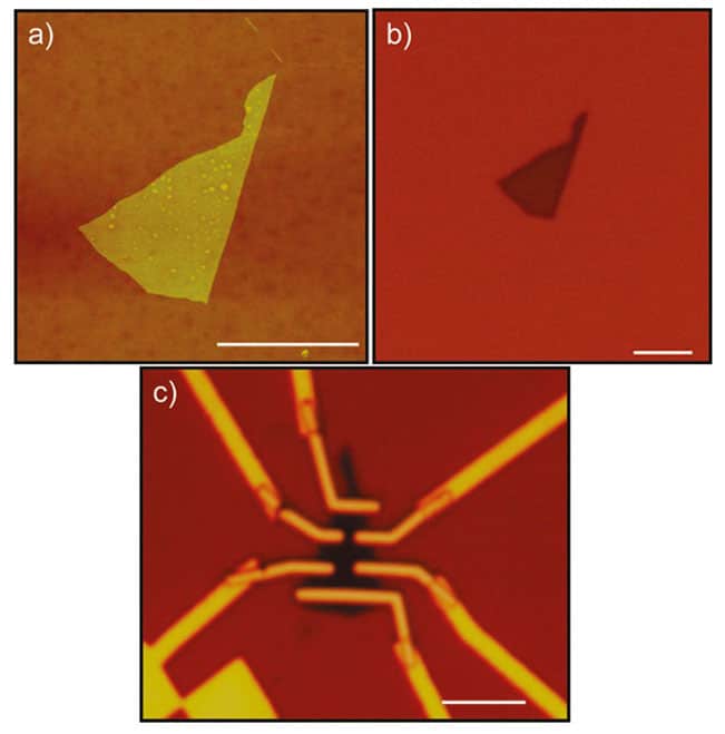
The Maryland researchers, who are at the Materials Research Science and Engineering Center, produced thin layers of Bi2Se3 by exfoliating (or mechanically peeling apart) thicker crystals of the material. Bi2Se3 is a layered material (like graphite) and easily cleaves to produce very thin pieces. They then made field-effect transistors from the material on a substrate of silicon dioxide over conducting silicon that then acts as the gate electrode for the devices.
The electron mobility of its ultrathin transistors is still quite low – around 10 cm2/Vs, which is much lower than that of silicon. According to the team, this value could be greatly improved, however, by epitaxially growing Bi2Se3 thin films.
“We are also looking at growing cleaner Bi2Se3 by molecular beam epitaxy and how to inject and detect spin currents in it,” says Fuhrer. “We are studying the sources of disorder in the material to improve its quality and are investigating the optical properties of thin Bi2Se3 in the infrared to understand its optoelectronic and optospintronic properties.”
The current results were detailed in Nano Letters.


