The first room-temperature, high-sensitivity infrared photodetector has been designed by a team of researchers in the US. The device is based on the “wonder material” graphene and works across the full infrared spectrum. The detector is thin, flexible and transparent, making it highly suitable for applications including wearable electronics, according to the team. The researchers are currently developing an infrared camera by building an array with their graphene photodetectors.
Graphene is a layer of carbon just one atom thick and since it was first isolated in 2004 its remarkable electronic and mechanical properties have been studied by physicists worldwide. Zhaohui Zhong, Ted Norris and colleagues from the University of Michigan have been developing photodetectors that can take advantage of graphene’s unique material properties, including its ultra-broadband light-absorption capability. As graphene is a semimetal, it is capable of absorbing light across a wide spectrum – from ultraviolet to far infrared. This is unlike conventional photodetectors, which are made from semiconductors that can only absorb light at specific wavelengths.
Across the spectrum
As well as in night-vision goggles, infrared detectors have a variety of other uses: they can detect heat leaks, monitor blood flow and identify certain chemicals in the environment. They can even be used to study paintings, looking through multiple layers of paint to determine older versions of an artwork. However, the detectors require a combination of technologies to accurately detect the whole of the infrared spectrum. Indeed, detecting mid-infrared and far-infrared radiation requires the sensors to operate at very cold temperatures, thus making them impractical for everyday use.
While graphene has been used previously to make photodetectors, these have been limited by their poor sensitivity. With its one-atom thickness, graphene only absorbs about 2.3% of the light incident on it. “The challenge for the current generation of graphene-based detectors is that their sensitivity is typically very poor,” says Zhong. “It’s a hundred to a thousand times lower than what a commercial device would require.” It is this sensitivity that the Michigan researchers’ design has hugely improved upon.
Graphene gain
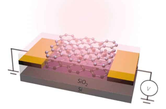
The device itself is made of two graphene sheets with a thin tunnelling-barrier layer between them. When light hits the top layer of graphene, it creates “hot” electrons and holes with high energy. “By designing the material interfaces properly, the hot electrons will tunnel through the barrier layer into the bottom graphene layer, while leaving behind positively charged holes on the top graphene layer,” explains Zhong. “The positively charged holes can produce an electrostatic gating effect and this affects the current readout of the bottom graphene layer.” Measuring the change in current allows the team to detect the brightness of the light incident on the detector. Rather than trying to directly measure the freed electrons, Zhong and colleagues configured the bottom-layer graphene as a field-effect transistor, which provides an intrinsic gain to amplify the tiny current and so overcomes graphene’s natural low sensitivity.
“We can make the entire design super-thin,” says Zhong. “It can be stacked on a contact lens or integrated with a mobile phone.” It can also be scaled down further, and so the team is currently working on making an infrared camera using an array made up of the detectors – Zhong says the prototype will be ready in a few years. He also foresees the use of their detectors in wearable applications because they could potentially be integrated into contact lenses or electronic eyes. “But for now, there are many fundamental scientific, material and engineering challenges that need to be addressed first. Making an infrared camera will be the first step,” says Zhong.
The research is published in Nature Nanotechnology.


