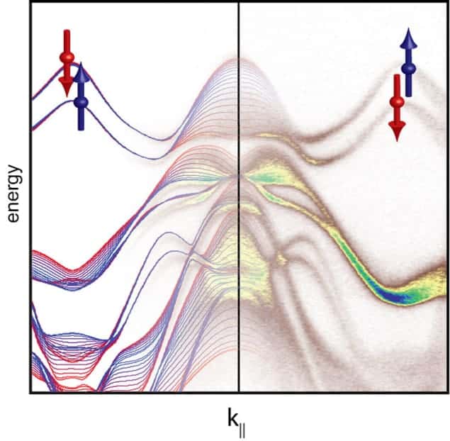
The first direct observation of giant spin-splitting has been made by an international team of researchers, which made the discovery while trying to develop spintronic technologies. The discovery came as a surprise because the material being studied – tungsten diselenide (WSe2) – has a crystal symmetry that, conventionally, would not allow for such spin-splitting to occur.
Spintronics is an emerging technology that aims at harnessing the electron’s intrinsic spin and magnetic moment to develop new kinds of solid-state devices that are much faster, smaller and more energy efficient than current electronics.
Giant spins
Such research has already paved the way to more advanced computer memories and hard drives. However to build transistor-like devices based on the electron’s spin alone, researchers must have a clear idea of how electron spins travel in a solid, as dictated by the underlying spin-dependent electron band structure of the material. In particular, it is important to create a material with large “spin-splitting” – the separation of the spin-up and spin-down states in energy and momentum – that can be switched on and off at will. Unfortunately, to date the splitting seen in candidate materials has been too small to have any practical applications.
Now, Philip King and Jon Riley at the University of St Andrews in the UK, along with colleagues in Europe, Japan and Thailand, have combined detailed experiments and theoretical calculations of WSe2 and have, surprisingly, observed giant spin-splitting in the material, even though the material’s structure suggests that any such splitting should be impossible.
The finding came as a shock because WSe2 is what researchers describe as a “spin-degenerate” material. This means that even though the electrons are subject to very strong spin–orbit interactions, the material’s crystal symmetry makes it nearly impossible to see the states clearly “spin-polarized” – that is, a clear split or segregation of the spin-up from the spin-down states. But this split is exactly what the researches saw. A WSe2 crystal comprises two alternating 2D atomic layers, and they found that each layer had almost 100% spin-polarized states. But this contradicts a fundamental symmetry known as “inversion symmetry” that WSe2 possesses. So what is going on?
Layered mystery
What King’s team ultimately found is that while WSe2 is spin-degenerate in its bulk, individual, atomic layers of the material are highly spin-polarized, where the inversion symmetry is broken. WSe2‘s overall crystal structure is that of many layers, with each layer rotated 180° relative to the previous one. Within each atom-thin layer, inversion symmetry is broken or not present, and the electronic states in that layer are highly spin-polarized. While this applies only to those electronic states that are restricted to a layer (some states are delocalized across multiple layers of the crystal), this includes the majority of the material’s states.
Overall inversion symmetry is maintained and the sign of the spin-polarization for states confined in one layer “is exactly compensated by that of the equivalent states in the rotated layer” says King. “So locally, the states are spin-polarized, while globally they are not, and the consequences of inversion symmetry are restored,” he says. King further explains that such materials where spin-polarized states are “already hidden away in the bulk” would be perfectly suited to exploitation for spintronics applications because the material has electronic states that are naturally spin-polarized – something that is normally induced in previous spintronics materials.
Unlocking potential
Splitting one layer of WSe2 from another, for example by applying a voltage difference between them, would “unlock the potential of this material for hosting large tuneable spin-splitting”, according to King, and could provide a very large spin-splitting of nearly 500 meV at a maximum. “This is because the spin-splitting would be directly tied to the energy difference between the two layers,” says King. Previously, the largest such splitting, which was also observed by King, along with other colleagues in 2011, was around 200 meV. This amount of splitting should make it possible to develop a small device that actually functions at room temperature, so 500 mV is even better.
King also points out another benefit of the WSe2 system in that the spin points out of the 2D layer of the system, while in previous systems, the spin tended to point in the surface plane of the material. This, he says, adds an “additional functionality to the spintronics tool box”.
To make its observations, the team selectively probed just the top layer of WSe2 by carefully tuning the measurement parameters. To do this, the team used a technique known as “angle-resolved photoemission spectroscopy”, and studied the samples at MAX-lab at Lund University in Sweden and the Diamond Light Source in the UK. This allowed the group to track propagating electrons in a solid. A beam of bright, monochromatic synchrotron light illuminates the sample, displacing electrons at the surface via the photoelectric effect, which are then scattered off a heavy metal surface. As electrons that are spin-up scatter in one direction, and those that are spin-down scatter in another, the researchers calculate where the two types of spins would scatter to, and place detectors. By then measuring the energy and the incident angle of the electrons, the team can reconstruct the energy splitting on the spin-up from the spin-down states.
King is excited by the possibility of a whole new class of such materials with “hidden” spin-polarization. “Controlling this could bring fantastic new opportunities for spintronics, and a large arsenal of new materials in which we can achieve this,” he says.
“One of the key contributions of this paper is to highlight the importance of the layered nature of this material by demonstrating that the spin properties can vary enormously from layer to layer,” says spintronics expert David Awschalom from the University of Chicago in the US, who was not involve in the new work. “Spin-splitting on this scale in a semiconductor is valuable for the prospect of spin-based logic, which has the potential to significantly impact high-speed, low-power electronics,” he says, further explaining that transition metals such as WSe2 “have exotic properties of their own, and physicists are just beginning to sort them out. What’s especially fascinating about this work is its focus on fundamental spin and electronic properties of a new material. And new material properties often catalyse new applications”.
The research is published in Nature Physics.
- To find out more about the basics of spintronics, take a look at our “Spintronics made easy” video.


