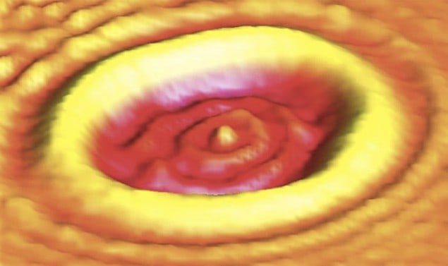
Images of relativistic electrons trapped in graphene quantum dots have been taken by physicists in the US and Japan. The ability to confine and control electrons in such a way could play an important role in developing graphene-based nanoscale devices and could also provide a better understanding of these exotic “Dirac fermions”.
Graphene is a honeycomb lattice of carbon atoms just one atom thick that was first isolated in 2004. It has a number of unique electronic properties, many of which come from the fact that it is a semiconductor with a zero-energy gap between its valence and conduction bands. Near where the two bands meet, the relationship between the energy and momentum of charge carriers (electrons and holes) in the material is described by the Dirac equation and resembles that of a photon. These bands, called Dirac cones, enable these charge carriers to travel through graphene at extremely high speeds approaching that of light. This extremely high mobility means that graphene-based electronic devices such as transistors could be faster than any that exist today.
Tunnelling problems
Despite the material’s many useful properties, there are still many challenges facing researchers trying to create graphene-based devices. One problem is related to the fact that the behaviour of charge carriers in graphene is governed by Klein tunnelling – a counter-intuitive effect in which relativistic particles can pass through a potential barrier with 100% probability. Because graphene’s charge carriers behave like relativistic particles, Klein tunnelling is therefore predicted to exist in potential barriers (p–n junctions) fabricated in the material.
“This exotic behaviour, albeit very interesting, makes trapping and controlling graphene’s charge carriers very difficult,” explains team-member Jairo Velasco Jr of the University of California, Berkeley, and the University of California, Santa Cruz. “It is, however, important for us to be able to map the behaviour of these Dirac fermions at p–n junction boundaries, to explore Klein tunnelling physics in the carbon material and to better control and confine the electrons in it.”
The researchers, led by Michael Crommie, created circular p–n junctions in graphene by positioning the tip of a scanning tunnelling microscope (STM) about 2 nm above the surface of a graphene sample while applying a voltage pulse to the tip. “While doing this, we also apply a constant voltage on a silicon slab that is below the graphene, but separated from it by a silicon-oxide capping layer and a boron nitride (BN) flake,” says Velasco. “The intense electric field emanating from the STM tip ionizes defects in the BN region directly beneath the tip and the released charge migrates through the BN to the graphene. This leaves behind a space-charge build-up in the BN that screens the electric field from the silicon slab.”
Mapping wavefuctions
The next step is to take an image of the Dirac fermions in the graphene sample. “To do this, we position our STM tip about [0.1 nm] above the graphene surface,” continues Velasco. “This allows us to measure a tunnelling current between the suspended STM tip and the graphene surface.” This measurement is a direct probe of the quantum-mechanical wavefunction of electrons in the carbon material. By moving the STM tip to different lateral positions on the sample, this allows the team to build-up an image of how the wavefunction varies inside and outside the circular p–n junction (see figure).
Until now, obtaining direct images of electron wavefunctions in graphene had been notoriously difficult. This was because the systems in which researchers were trying to observe them – lithographically patterned structures, graphene edges and chemically synthesized graphene islands, for example – contained too many defects.
Mark Fromhold of Nottingham University in the UK, who was not involved in this work, says that defects are “often problematic in solid-state devices because they produce unwanted electrical or optical behaviour. But in this beautiful new experiment, the Crommie group has shown how defects can be used, together with a scanning probe, to overcome a major challenge in graphene physics, namely how to stop electrons leaking through p–n junctions by Klein tunnelling. Not only did the researchers manage to confine the electrons in a quantum dot created in the graphene layer, but they were also able to directly map both the resulting energy-level spectrum and the corresponding quantum wavefunctions.”
Quantum dots
According to Velasco and colleagues, the techniques developed in this work could now be used to study more complicated systems as well, such as multiple quantum dots with arbitrary geometries. “This is because the graphene circular p–n junctions we made (which can be considered as quantum dots too) are fully exposed, and so we can directly access them with real-space imaging probes,” Velasco says. “This is completely different to conventional semiconductor quantum dots, which are generally inaccessible.”
The team, reporting its work in Nature Physics, says that it now also plans to investigate bilayer graphene, which hosts massive Dirac charge carriers. “These charge carriers are expected to completely reflect upon impinging on a p–n junction barrier, independent of the barrier width.”
The same issue of Nature Physics also contains a paper by Christopher Gutiérrez of Columbia University and colleagues who have also obtained images from electrons trapped in a graphene quantum dot.
- A version of this article first appeared on nanotechweb.org


