The opportunity to carry out academic research backed up with the resources of industry attracted James Endicott to electronics company e2v

While studying for my undergraduate degree at the University of Nottingham in the UK, I developed a strong interest in condensed matter physics. This led me to undertake a PhD in semiconductor physics and then, almost before I knew it, I was starting my final year and contemplating what to do next. Although the PhD was a great experience, after many years following an academic path I felt it was time for a change. I started looking for industrial jobs with a focus on engineering and physics, and quickly discovered e2v – a leading design firm of electronic components and subsystems. I applied for the company’s annual graduate scheme in 2005 and was delighted to be offered a job working with charge-coupled devices (CCDs).
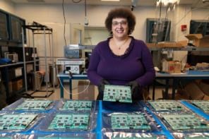
e2v manufactures electronic tubes, sensors and semiconductors for the medical, scientific, aerospace, defence, industrial and commercial sectors. The company employs about 1800 people across three manufacturing sites in the UK (Chelmsford, Lincoln and High Wycombe) and a fourth in Grenoble, which was recently acquired from a French electronics company. Although the name e2v is only a few years old, the firm was started 60 years ago as the English Electric Valve Company.
Sensors in space
CCDs are arrays of capacitors made from semiconductor materials that are used in a variety of digital-imaging applications, from mobile-phone cameras to telescopes. The CCDs designed and manufactured by e2v have historically been closely associated with the space industry. For example, its CCDs have been chosen by NASA and the European Space Agency for major research missions including the Hubble Space Telescope and the Mars Reconnaissance Orbiter. For such missions e2v has developed sensors not just for imaging but also for spectroscopy and guidance systems.
In addition to space projects, e2v makes CCDs for several other market sectors. In medical imaging, for example, its sensors are used in X-ray and biopsy analysis. Scientific applications include spectroscopy, microscopy, fluoroscopy and crystallography. And its patented “L3Vision” system allows CCDs to be used in very low light conditions, leading to industrial applications such as night-time surveillance cameras.
Since starting at e2v, I have mainly worked as a device development engineer. Initially, this involved some simple testing and experimental work, but I soon began a project in which I modelled the circuits that are used in CCDs to detect electric charge. Recently, I have taken on some investigative projects associated with the wafer fabrication process of the CCDs. My aim here is to improve the manufacturing yield and ensure that the firm will be able to cope with the next generation of device designs. In addition, I have started a secondment in e2v’s product-engineering group. Product engineers are responsible for testing and evaluating devices, and ensuring that the product is delivered to customers on time. This role requires a good understanding of the devices, as the engineer must interpret test data, solve problems and respond to customer queries.
Solving problems
My work at e2v has been varied and interesting, with a mix of hands-on practical experience together with analytical and investigative research. From a technical perspective, there is always something new to learn about the devices, be it in the operation, application or manufacture. There are certainly similarities between the experimental work I undertook during my PhD and the practical problem solving that is involved in the job of an engineer at e2v. In both cases, the challenge is to get a result from your equipment in the best possible way. Other skills that I developed at university, such as the ability to communicate clearly and write concise reports, have also proved invaluable in the work place.
I have found the main difference between industry and academia to be the level of support available to me. As a PhD student you often struggle to find resources and so have to be creative in finding solutions to your problems. In contrast, in industry, the commercial pressure of satisfying the customer means the support available is much greater. The implementation of milestones and targets at the company also makes the pace of the work faster than while doing a PhD.
Most new starters working on CCDs are physics graduates who join the product-engineering group. There is a healthy balance of people with undergraduate and postgraduate qualifications from a wide variety of universities. In this role, new starters can make use of their physics degree while they get up to speed with the CCD aspects of the business and learn the importance of their work to the customer.
Physicists who have started in the product-engineering group have moved on to a wide range of roles. Some have stayed within the group to become senior engineers who are experts in their chosen technology. Others have moved into applications engineering, where they work closely with the customer to bid for contracts for new business. Alternatively, some engineers have progressed to managerial roles such as team leader or project manager, with a host of new challenges and responsibilities. Whichever path you choose to follow, in a company such as e2v with a broad product portfolio and a vision to expand, the prospects are bright.