As AI pushes conventional silicon computing towards its physical and energy limits, researchers are exploring radically different ways to process information – from magnetic bits and in-memory logic to optical and brain-inspired machines. Sidney Perkowitz investigates how physics could reshape the future of computation
Modern computation ranks among the great technical achievements of the 20th and 21st centuries and touches nearly every area of human activity. Today digital computing uses billions of transistors etched onto semiconducting silicon chips to work as tiny switches that represent binary 0 or 1. The technology underlies personal phones and laptop computers, and extends to supercomputers that perform nearly one quintillion operations per second (1018 floating point operations per second, or FLOPS) and manipulate up to 100 petabytes of data.
Supercomputers can simulate otherwise intractable problems in science, from climate and weather patterns to protein folding and even black-hole interactions. However, further progress in scientific and general computation is approaching saturation because of fundamental limits, while the explosion in artificial intelligence (AI) based on large language models (LLMs) is clearly showing where computation needs to be improved. Physics is essential for this effort.
Nearing the physical limits
Back in 1965, Intel co-founder Gordon Moore famously predicted that the number of transistors we could fit onto a silicon chip would increase exponentially. He later forecasted that the number would double roughly every two years. Moore’s law has held for decades, albeit at a lower rate since the mid-2010s. More transistors meant increased computing power per chip, as well as faster computing.
That’s because smaller transistors switched between binary states more quickly, and higher transistor densities reduced the distance signals had to travel. These factors made it possible to increase “clock speed” – the frequency at which a computer’s central processing unit (CPU) synchronizes its internal operations – which helps determine computational speed. That frequency grew from tens to hundreds of megahertz in the 1970s–1990s until it reached gigahertz levels.
Moore’s law: further progress will push hard on the boundaries of physics and economics

But by the early 2000s, the increase in clock speed with density of transistors no longer held. Transistors that switched more frequently used more power, generating heat beyond what could easily be dissipated. Essentially, clock frequencies have stagnated at 3–5 GHz.
Within this limitation, the strategy for faster computing has been to design chips for parallel processing. Modern CPUs contain “cores”, which are separate processing units on a chip that independently read and execute instructions. In a CPU with four cores, each operates at the clock rate of 5 GHz, say; but since they operate in parallel, the throughput can approach a fourfold increase.
Another, more specialized form of parallel processing was introduced in graphics processing units (GPUs). While a CPU typically has between four and 32 powerful cores that have been optimized for flexibility in carrying out different tasks, a GPU has hundreds to thousands of simpler cores, designed to deal with many data elements for such tasks as rendering images or multiplying large matrices.
GPUs have become essential for supercomputers, but they also face limits. Trouble is, not all computational tasks can be broken into parallel operations, while adding more transistors to a chip still requires more power and generates yet more heat.
Large scales and rising costs
Supercomputer-level capabilities, however, are needed to support the rising use of LLMs such as ChatGPT, which are trained on huge data-sets and can create content based on natural language. Other LLMs followed, and by 2025 up to a billion individuals, corporations and governments were using AIs globally. This enormous scale of usage is highly demanding of computational and electrical power.
LLMs need two kinds of computation. First there is training computation, which analyses massive amounts of text from books, articles and websites containing trillions of tokens – words or parts of words. The training’s aim is for the model to learn statistical patterns in a given language, and estimate the probabilities for the next token in a given sequence.
Training the largest LLMs can take up to 100,000 GPUs using tens to hundreds of megawatts, comparable to the biggest supercomputers. A few dozen of these centralized installations are estimated to be operating around the world, concentrated in the US and China.
The second type of computation is inference, where an already trained model responds to user prompts. Inference processing needs less computational and electrical power, but runs continuously to serve users. It must also respond with little latency, the time delay between request and response, so inference infrastructure is geographically distributed, not centralized.
How AI can help (and hopefully not hinder) physics

Of about 12,000 general data centres operating globally, hundreds to a few thousand now support a large AI cluster for inference, with the number rapidly growing. With this scale of continuous operation, inference is expected to dominate long-term AI energy use.
By 2030, global data centres, driven largely by AI, are expected to consume some 1000 TWh per year, corresponding to an average load of roughly 100 GW. This is a few percent of global electricity use and the resulting waste heat must be removed, requiring millions of gallons of water for some facilities. This heat discharge, along with the necessary additional electricity generation, will have a significant impact on the environment.
That’s provoked reactions to AI infrastructure, both from communities objecting to local data centres and governments concerned about national power grids. Scaling today’s relatively few specialized supercomputers to many large AI centres around the world carries significant costs, not to mention AI’s uncertain societal impact. As AI stretches resources, researchers are keen to rethink the very nature of computation.
Building a better bit
The use of electronic circuits to carry out binary logic, which defines modern computation, was mathematically formalized by the US mathematician Claude Shannon. In 1937 he showed that on/off electrical switches, arranged in what we now call a “logic gate” (based on the true/false logic George Boole invented in the 19th century), can carry out arithmetic as well as logical decision-making.
This approach has been embodied in computers, first using electromechanical relays, then vacuum tubes, followed by discrete transistors, and finally CMOS (complementary metal-oxide-semiconductors) integrated circuits. Each succeeding generation has slashed the energy required for a single binary switching event – for example, from nanojoules for an older discrete transistor to femtojoules for a transistor in a modern CMOS chip.
But this gain has been far outstripped by the rapidly growing volume of computation. Despite improved energy efficiency, our increasingly computerized world demands more electrical energy. Fortunately, there are other, more efficient ways to encode binary information using physical systems that support two stable states: the horizontal or vertical polarization of a photon; the up or down orientation of the spin magnetic moment of an electron; or persistent superconducting currents circulating in opposite directions.
Each approach has its own advantages and drawbacks. Photon-based computing offers high speed and reduced resistive heating; but it is difficult to store photons. Superconducting currents offer high speed, and require low energy per operation. But the energy cost for cryogenic cooling at 4 kelvin, hundreds of watts per one watt of heat removed, diminishes or wipes out the energy advantage.
“Spintronics” technology, however, has been the most successful of the three. Its basic device is the magnetic tunnel junction (MTJ), where a thin insulating barrier separates a “reference” and a “free” magnetic layer. The device’s electrical resistance depends on whether the magnetizations of the layers are parallel or antiparallel.
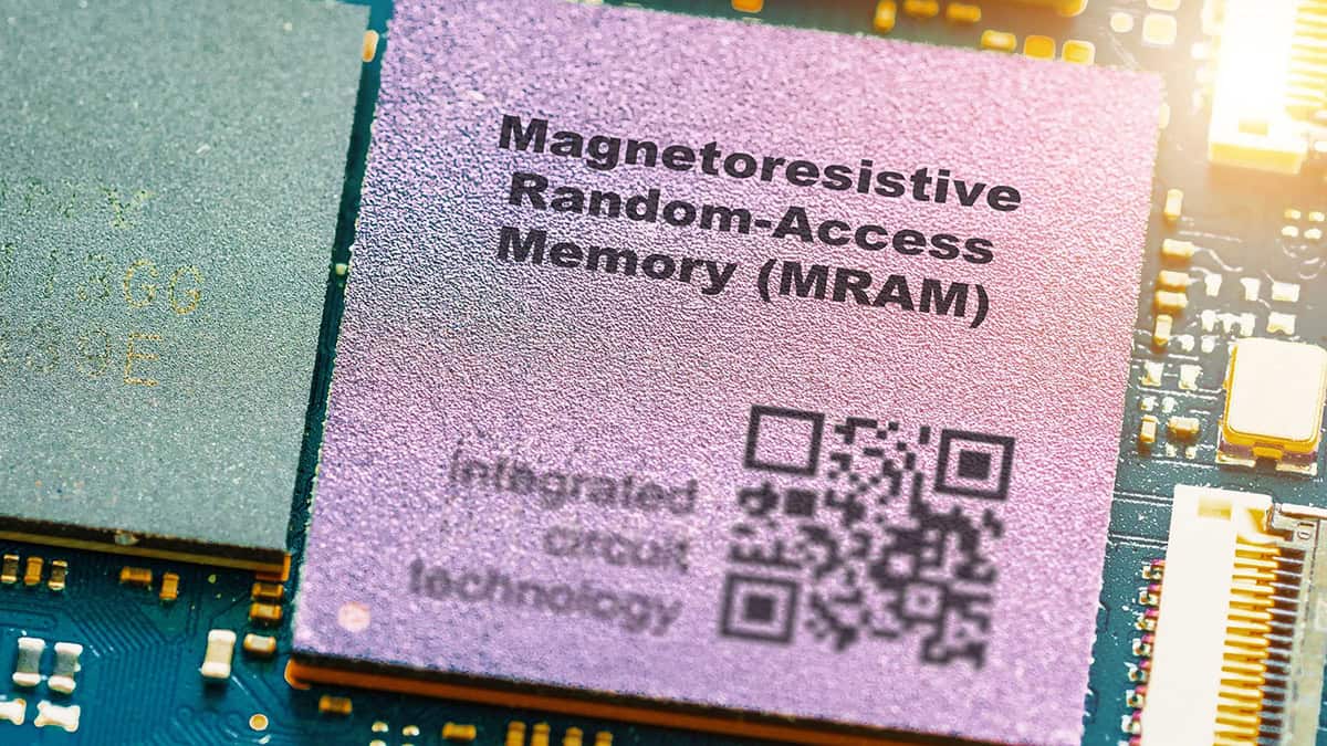
MTJs exist in hard disk drives and can also serve as read-write units in a magnetoresistive random-access memory (MRAM). To read, a small current is passed through the MTJ, and the resulting voltage shows the state of the bit. To write, a larger current is applied. The fixed layer polarizes the spin of the electrons, which carry angular momentum as they tunnel into the free layer.
This flips that layer’s magnetization, switching the magnetic bit, whose state survives even without power. That’s a key advantage of MRAMs compared to volatile CMOS RAMs, which require power and lose their stored data without it. MRAMs are not yet competitive with CMOS RAMs, but are already used in automotive, aerospace and other applications where their non-volatile nature is essential to reduce power needs and maintain their data under extreme conditions.
Along with this benefit, new possibilities for spintronics are emerging. In 2024 Nuh Gedik at the Massachussetts Institute of Technology (MIT) and colleagues reported that they had rapidly induced magnetism in iron phosphorus trisulfide with light (Nature 636 609). FePS₃ is an antiferromagnet where atomic spins in opposite directions result in little or no net magnetic field. The researchers found that picosecond pulses of terahertz light produced magnetic states that persisted for milliseconds – far longer than any other reported light-induced magnetism (see box below).
Metastable magnetization
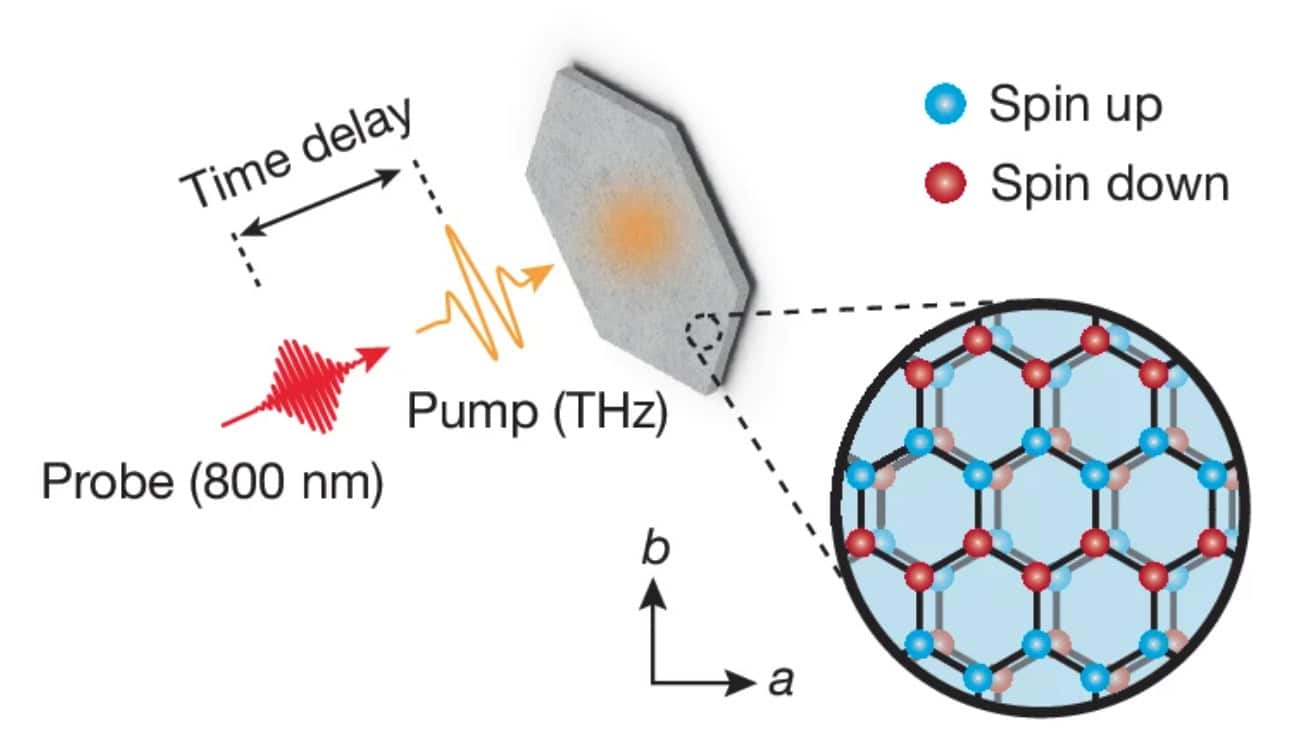
Shown here is the experimental set-up that an international team of physicists use to produce a long-lasting, light-driven magnetic state in a material such as iron phosphorus trisulfide (FePS3), which becomes antiferromagnetic when cooled below about 118 K. They used an intense terahertz-frequency (THz) pulse (orange) to drive low-energy collective excitations, which induce transient changes in optical properties that can be probed with an 800 nm probe pulse (red). Fe2+ ions form a hexagonal lattice and their spins arrange ferromagnetically along the zig-zag chain (a-axis) and antiferromagnetically between the adjacent chains (the structure in the circle). The magnetic coupling between the layers is antiferromagnetic together with a small interlayer shear distortion along the a-axis. The THz pulses put the material in a metastable magnetic state that lasts for more than 2.5 milliseconds even after the light source is switched off.
Earlier this year, researchers at Beijing Normal University in China found that light-induced magnetic transitions consume little energy (ACS Nano 20 9051). If magnetic bits become competitive with electrical ones – activated by light or otherwise – they would unite working memory and long-term storage in one computational stage rather than two as we now have. Magnetic bits could also play a role in a bigger change in computer structure.
Bringing it all together
A novel form of computer architecture could also remove a famous bottleneck in computing that dates back to the influential 1945 proposal by the mathematician John von Neumann for a general computational design. He suggested using separate processing and memory (first put forth in 1837 by Charles Babbage for his mechanical “Analytical Engine”) but added the idea of the stored program.
By holding the instructions for computer operations in memory along with data, a computer program makes computation more flexible but has one big drawback. Data and instructions have to shuttle between processor and memory along the same channel, reducing computing throughput and using more energy than processing – the “von Neumann bottleneck”.
Novel computing: liquids, soft solids and deuterium
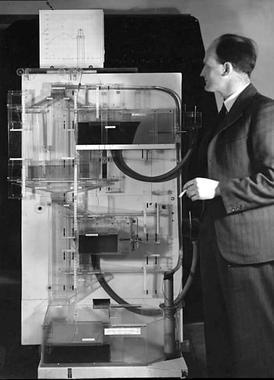
At the heart of modern computing technology are ultra-pure silicon wafers. These nearly perfect regular crystalline solids form the substrates for integrated circuits, making it all the more surprising that less ordered materials – such as liquids and soft solids – have their own history in computation.
In 1949, for example, the UK-built Monetary National Income Analogue Computer (MONIAC) simulated the flow of money within a national economy using coloured water moving through transparent tubes under gravity. Water levels representing economic conditions were set by pumps and valves. As the water negotiated the system, it dynamically illustrated how parameters such as tax rate affect an entire economy, eventually settling into equilibrium.
Another liquid – mercury – also appeared in the early days of electronic computing. The first commercial unit in the US, UNIVAC I (1951), stored nine kilobytes of data as sound pulses continually recirculating in tubes filled with liquid mercury acting as delay lines. The units, which were bulky and heavy, provided serial rather than random access because the pulses travelled in sequence. Timing was crucial, and the mercury was held at a constant 40 °C to keep the speed of sound stable. Another early computer, EDVAC, also stored data in liquid mercury.
Since the 2000s researchers have shown that tiny droplets of oil, moving through small channels filled with water, can implement binary logic. If a droplet blocks a channel, a second droplet arriving behind it is diverted into another channel, representing a “decision”. Proper design can emulate the Boolean logic that underlies conventional computing. With channels only 100–200 µm across, microfluidic logic could route and process small samples, providing a lab on a chip for chemical analysis, biological research or medical diagnostics.
Yet another liquid – one more exotic than mercury – and a soft solid were apparently at least considered for computation in the same era as UNIVAC 1. According to Iain Dey and Douglas Buck’s 2017 biography The Cryotron Files: the Strange Death of a Pioneering Cold War Computer Scientist, the MIT scientist Dudley Buck once worked on a data storage system using magnetic pulses in liquid deuterium held at cryogenic temperature. In that Cold War era, US government money was available for any research that might help America and the authors describe how some of it also went on studies into a soft, wobbly foodstuff, lemon Jell-O as well as the viscous semi-liquid hair preparation Wildroot Creme Oil, which might also support sound waves in a memory unit. None of this Cold War research panned out, although at least the Jell-O experiments could treat the entire lab team to dessert.
One solution is to carry out processing and memory functions in the same physical element, potentially using a new type of electric circuit element originally proposed in 1971 by the US electrical engineer and computer scientist Leon Chua. Its resistance depends on the accumulated charge and, since charge is the time integral of current, therefore carries a memory of the device’s past electrical activity.
Chua dubbed his new element a memory resistor or “memristor” – and the concept can be used when a read-write MTJ holds a memory of past electrical activity as a magnetic bit. In 2026 Shahar Kvatinsky at the Israel Institute of Technology and colleagues showed that small MRAMs formed from MTJs can perform logical operations inside memory (Adv. Electron. Mater. 12 e00348).
In principle, therefore, this could also provide arithmetic processing inside memory, thereby removing the von Neumann bottleneck. The non-volatile memory would also save energy relative to CMOS memory. Problems remain though, such as reducing noise and producing large-scale MRAMs – but the ability to merge memory and computation within MRAMs has been established at small scales.
Certain material structures can also play a dual function. The wonder-material graphene – a 2D hexagonal lattice of carbon atoms – is electrically conductive when a voltage is applied in its plane, driving the electrons. If the graphene sheet is also placed between proton-conducting electrolytes, a second voltage applied across the sandwich produces a proton current (a flow of positive charge) perpendicular to the plane.
In 2024 Marcelo Lozada-Hidalgo at the University of Manchester and colleagues found that certain values of electron density in this structure make the graphene an insulator (Nature 630 619), producing a reversible change from conducting to insulating that forms a non-volatile two-state memory. Their set-up allowed the researchers to perform logic and memory operations in a single device for the first time.
As graphene, MRAMs, and other approaches are under study for in-memory computing, another method emulates a natural process – and is perhaps the biggest departure from conventional computing.
Dual purpose
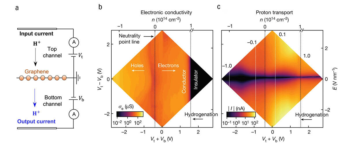
(a) Graphene is well known to be a good electrical conductor, but in 2024 an international team of researchers used the 2D substance to make a new electrically-controlled switching device that supports both memory and logic functions. The device exploits graphene’s ability to conduct protons as well as electrons. The team showed that placing a sheet of it between proton-conducting electrolytes also produces a proton current perpendicular to the plane, with the proton and electron transport allowing independent control of field and charge density. Shown here are the top and bottom voltages and the direction of electron and proton flow. (b) Map of in-plane electronic conductance, σe, as a function of electric field E and charge density n. The left and bottom axes show that these variables are controlled by the difference and sum of the top and bottom electron voltages, respectively). (c) Map of proton transport current, I, as a function of E and n.
Copying biology
In the 1980s, Carver Mead – a Caltech physicist and engineer who had been instrumental in developing integrated circuits and deeply understood the physics of computing – made a radical proposal. Instead of building computers around centralized digital logic, we should instead design them to imitate the strategies that make the human brain highly efficient. He coined the term “neuromorphic” computing for this approach and is widely considered its founder.
Smarter machines: the evolution of neuromorphic engineering

Using specific biological and biophysical features, the brain performs its cognitive and sensory tasks at the modest power of 20 watts. Its 86 billion neurons do not constantly use energy, but act sparsely in response to events, firing brief electrical spikes at definite timings and rates. A system like this can be expected to save energy compared to a conventional computer, which steadily consumes energy at the CPU clock rate.
Also, there is no von Neumann bottleneck in the brain. Information is stored as changes in synapses: the ~1014–1015 connections among neurons that control signal flow. As a spike arrives, a synapse immediately applies its stored information. The modified signal is passed on to neurons that repeat the cycle. Storage and processing occur together within this closely linked 3D network, which also operates in a massively parallel manner.
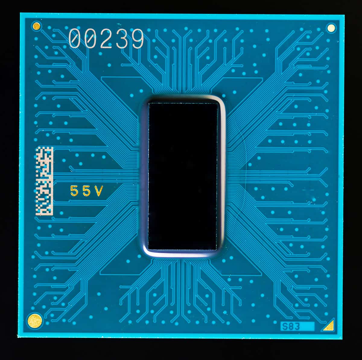
Mead had envisioned an analogue neuromorphic design, but in practice the biological features are expressed digitally to match CMOS technology. For example, in 2017 Intel introduced its Loihi chip with event-driven spiking and closely connected computation and memory. A later model was reported in 2025 (arXiv:2503.18002) that trebled the throughput for matrix multiplication – the main computationally-intensive operation needed to train an LLM – with half the energy a standard GPU chip uses.
Similarly, in 2014 IBM built and tested a chip that emulated spiking behaviour, while a later version, dubbed NorthPole, does not use spiking. In 2025, meanwhile, IBM researchers reported that 288 linked NorthPole chips could carry out AI inference on certain sizes of language models at favourable speeds and power usage.
The future of computing and AI
Most of the novel approaches are in the proof-of-principle or pre-commercial phase and may never reach wide use, for both economic and engineering reasons. The investment in CMOS technology and the associated computer architecture is enormous. Any overall change would be a massive undertaking. Although a neuromorphic chip might be more efficient, it would require huge investment to be formally adopted by today’s markets and chip-making industry.
Even so, there are valuable lessons to be learned from the research into novel approaches – such as better integration of memory and computation. There is also a consensus that hybrid solutions can yield immediate benefits. An accelerator unit, such as a bank of neuromorphic chips, integrated with CMOS technology, could increase speed and decrease power use for the critical matrix multiplication stage. Upgrades like these can be included as new supercomputers and AI centres are being built, improving general and AI computation and reducing their energy costs.
We should also think of the problem from the other end: yes, we can now produce a form of AI based on LLMs. But this is ultimately a brute-force approach that demands a great deal of time, money and resources. It should continue to be refined, but there should also be space for bold ideas that may lead to better and more sustainable forms of AI, and of the computation it requires.