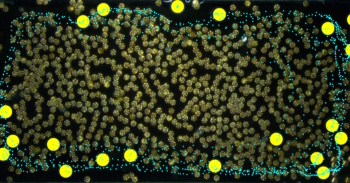
Researchers in Germany and Australia have grown two-dimensional materials directly on optical fibres for the first time, creating a new hybrid platform with possible applications in a host of optoelectronic devices, including photodetectors and non-linear light converters.
In their work, team members led by Falk Eilenberger, Andrey Turchanin and Antony George of the University of Jena and Markus A. Schmidt of the Leibniz Institute of Photonic Technology focused on a family of crystals known as transition metal dichalcogenides (TMDCs). These materials have the chemical formula MX2, where M is a transition metal such as molybdenum or tungsten and X is a chalcogen such as sulphur, selenium or tellurium. In their bulk form, TMDCs act as indirect band-gap semiconductors. When scaled down to monolayer thickness, however, they behave as direct band-gap semiconductors, capable of absorbing and emitting light at high efficiencies.
This property means that TMDCs in their 2D form are attractive building blocks for devices such as light-emitting diodes, lasers, photodetectors and solar cells. They could also be used to make circuits for low-power electronics, sensors or flexible electronic devices, and combining them with optical fibres could lead to further applications in non-linear optical devices and quantum technologies. But there is a catch: the task of transferring fragile, atomically-thin layers of material onto optical fibres is far from easy, and until now it had to be done manually, layer by painstaking layer.
The best of both worlds
The breakthrough came when the team, which also includes scientists from Sydney Nano, the Fraunhofer Institute for Applied Optics and Precision Engineering IOF and the University of Adelaide, developed a new growth process for 2D TMDCs. “By analysing and controlling the growth parameters, we identified the conditions at which the 2D material can directly grow in the fibres,” Turchanin explains. “The technique is based on chemical vapour deposition at a temperature of 700°C, which while high does not affect the properties of the optical fibres, which are heat-resistant up to 2000°C.”
The hybrid platform “combines the best of both worlds”, George says. The tiny thickness of TMDCs and planar substrates, he explains, means that the length over which light and matter can interact is usually restricted to less than a nanometre. This short interaction length reduces both the optical response of the TMDCs and the types of applications possible. Although coupling the TMDCs with optical resonators enhances the light-matter interactions, this strategy is limited to narrowband resonance, meaning that broadband, ultrafast operation remains challenging. In contrast, integrating TMDCs directly onto waveguides or optical fibres greatly increases the interaction length, even for broadband light.
While previous attempts at integration proved unsuitable for large-scale applications, the new technique overcomes this limitation. Growing the 2D materials directly on the optical fibres is a scalable process that, in effect, turns the fibres into 2D-functionalized waveguides, and produces interspersed monolayers of high-quality TMDC crystals that are around 20 microns long on fibres few centimetres in length.
Potential application areas
According the team, there are two main areas where the new hybrid system could find applications. The first is gas sensing. Here, the light-emitting properties of the TMDC would change as a gas is absorbed onto the functionalized fibre, leading to a change in the colour of light in the fibre. Since the fibres are so thin, a gas sensor based on this technology might be suitable for biotechnology or medical applications, the researchers say.
Why do we need new types of optical fibres?
Another possible application would be to use the composite optical fibres as nonlinear optical converters, capable of transforming laser pulses into white light for spectroscopy. The Jena researchers also mention applications in quantum electronics and quantum communication. “These applications would exploit the tendency of TMDCs to form single photon emitters around point defects or their large nonlinearity for spontaneous parametric conversion,” Eilenberger tells Physics World.
The researchers, who report their work in Advanced Materials, attribute their success to the “diverse expertise” in their highly interdisciplinary team. They have filed a patent application for their invention, and now plan to optimize the light-matter interaction by tuning the fibre’s geometry before demonstrating a sensing application with their platform.


