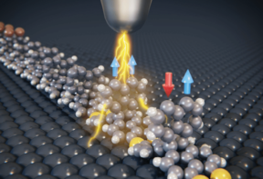
Graphene nanoribbons (GNRs) have many possible uses in electronics and optoelectronics, but a lack of efficient methods to prepare these ultra-narrow strips of carbon has so far limited their applications. Researchers in China and the US have now found a novel solution. By squashing carbon nanotubes in a diamond anvil cell, the team produce sub-10-nm-wide semiconducting GNRs with atomically smooth closed edges and few defects, potentially paving the way to a more widespread adoption of the material.
In its standard form, graphene (a two-dimensional sheet of carbon) is a semimetal with no gap between its conducting bands. One way of transforming it into a semiconductor with a bandgap – a necessary step before devices made from it can be switched on and off – is to reduce its dimensionality still further by making it into GNRs. Indeed, studies have shown that GNRs less than 10 nm wide are all semiconducting. Better still, GNRs with a width of 5 nm or less have a bandgap big enough to meet the requirements of high-performance logic devices.
The catch is that the electron transport properties of GNRs depend strongly on the smoothness of their edges. Any slight roughness will make the electrons scatter, thereby lowering the nanoribbon’s electron mobility. And unfortunately, high-quality, ultra-narrow GNRs are hard to make, especially if their edges need to be smooth along the entire length of a long ribbon.
Top-down and bottom-up
Strategies for making GNRs less than 10 nm wide fall into two categories – top-down and bottom-up. Examples of top-down strategies include: using ultrasound to exfoliate expandable graphite; starting with wider GNRs and slimming them down with gas-phase etching; using a nanowire mask to create narrow, strip-like patterns in two-dimensional graphene; and lithography guided by a scanning tunnelling microscope.
The trouble with these methods, explains Changxin Chen, a researcher at China’s Shanghai Jiao Tong University who led the new study, is that they tend to produce GNRs with rough edges and lots of defects, which substantially reduces the structures’ electron mobilities. “The non-uniform edges between the GNRs also result in large variations in the GNRs’ electronic structure and properties,” he adds.
Bottom-up strategies, for their part, include synthesizing the nanoribbons from solution or using a technique called surface-assisted assembly. Unfortunately, nanostructures created using these strategies also suffer from low carrier mobility, and they are typically short, just dozens of nanometres long.
Smooth edge-closed nanoribbons narrower than 5 nm
In contrast, the new top-down technique developed by Chen and colleagues creates atomically-smooth, edge-closed nanoribbons as little as 1.4 nm wide – the narrowest so far reported in GNRs fabricated using a top-down approach. “The prepared nanoribbons also boast sizeable bandgaps and high carrier mobilities, making them ideal for fabricating high-performance electronic and optoelectronic devices such as field-effect transistors,” Chen tells Physics World.
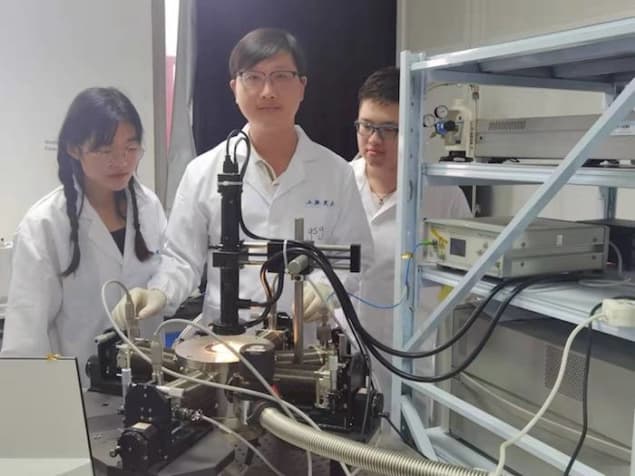
To make their GNRs, the researchers subjected single- and double-walled carbon nanotubes (CNTs) to pressures of as high as 22.8 GPa in a diamond anvil cell. After loading the CNTs into a sample chamber at the centre of a pre-indented tungsten gasket, they compressed the gasket between two anvils, heating the ensemble up to 220 °C for the highest pressures. Using in-situ Raman spectroscopy through the (transparent) diamond window of the cell, they observed that the electronic structure of the CNTs changed before and after the high-pressure/thermal treatment.
How to engineer topology in graphene nanoribbons
The researchers found that this method has a relatively high yield, transforming up to 54% of the starting material into edge-closed nanoribbons. The same method can also be used to fabricate edge-opened nanoribbons using nitric acid as an oxidant to selectively etch the edges of the squashed nanotubes. The technique could even be extended in other ways – for example, to make nanoribbons from other nanotube-forming materials or to flatten other fullerene materials.
Scaling up GNR synthesis
To test the electronic properties of their GNRs, Chen and colleagues made a field-effect transistor from a 2.8-nm-wide edge-closed nanoribbon. They found that it had an on/off current ratio of more than 104 and a sizeable bandgap of around 494 eV. It also had a field-effect mobility as high as 2443 cm2/V/s and an on-state channel conductivity of 7.42 mS.
The researchers say they are now trying to decrease the pressure required to squash CNTs by adding a “deviatoric” stress component or by regulating the temperature at which the thermal treatment is carried out at the highest pressures. “By using lower pressures, and thanks to our method’s high yield, we will be able to scale up the synthesis of the GNRs by using a multi-anvil approach or a large-volume press,” Chen says.
The technique is detailed in Nature Electronics.


