Two independent groups of physicists have shown that the topology of the electronic states of graphene nanoribbons can be controlled by adjusting the width of the material. Both teams made nanoribbons that alternated between wide and narrow sections and then showed that sections with different widths have different topologies.
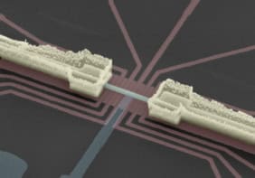
Graphene is a sheet of carbon just one atom thick that was first isolated in 2004. It has since been shown to have a wide range of fascinating and potentially useful electronic properties. In this latest research Daniel Rizzo, Gregory Veber and Ting Cao and colleagues at the University of California, Berkeley – and an independent team including Oliver Gröning and Shiyong Wang of EMPA in Switzerland and Xuelin Yao of the Max Planck Institute for Polymer Research in Germany – created graphene nanoribbons that were nine or fewer atoms wide. Crucially, the nanoribbons were defect-free – particularly at the edges, where the carbon atoms had the distinctive “arm-chair” configuration. In both cases, the widths of the nanoribbons varied by just two atoms from a narrow section to a wide section (see figure).
The nanoribbons were made to investigate whether they behaved as topological insulators. Such materials are electrical insulators in the bulk but conduct electricity like metals on their surfaces. This property can arise from the interaction between the spin of an electron and its motion, making it impossible for electrons to scatter when moving on the surface of a material.
Conducting point
In 2017, Steven Louie – who was part of the Berkeley team – calculated that graphene nanoribbons can be topological insulators. Because it is so narrow, a nanoribbon is essentially a 1D structure and this means that its topologically conducting surface is a zero-dimensional (0D) point that behaves like a conducting metal. This point contains just one conduction electron, which, despite its name cannot move. However, if another 0D point is nearby, electrons could quantum-mechanically tunnel between these points.
In their calculations, Louie and colleagues showed that the topology of graphene nanoribbons can change according to nanoribbon width. The also showed that the 0D metallic points can occur at the boundaries between regions with different widths, and therefore different topologies.
Now, the Berkeley and EMPA/Max Planck groups have confirmed that these metallic points exist. Also, by fabricating long nanoribbons with regions of alternating topology, both teams were able to engineer systems that are described by the Su-Schrieffer-Heeger (SSH) model. This was first developed in the 1970s to describe organic conductors and predicts that gapless topological states should exist at both ends of nanoribbons that alternate in thickness.
Qubit array
As well as being of fundamental interest to physicists, these topological states in nanoribbons could have technological applications. The spins of individual electrons trapped at 0D points along a nanoribbon could be used as a 1D array of quantum bits (qubits) of information. This could be used to create quantum computer in which information is processed by having the electrons tunnel from one site to another.
Another possibility is that topological superconductors could be made by putting the nanoribbons next to a superconductor.
The research is described in Nature: Rizzo et al and Gröning et al.