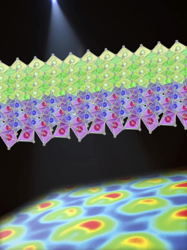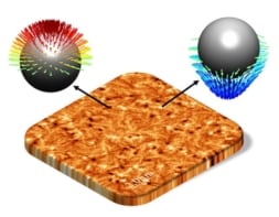
Scanning transmission electron microscopy (STEM) can be used to detect electric charge density as well as image atoms. This new advance comes from researchers at the University of California, Irvine, who used the technique to show how interfacing a ferroelectric oxide with an insulating oxide can produce an electron-rich region in between the two materials. The work is an important step towards understanding and engineering material structures with strongly-correlated electrons.
Nearly all the physical properties of materials are determined by how electron charge is rearranged between nuclei when atoms aggregate together. Being able to directly visualize how electrons are distributed is therefore important. Compared to other diffraction methods, aberration-corrected STEM (AC-STEM) allows for atomic-scale imaging of a sample using an electron beam, or probe, focused to about half an angstrom in size. When electrons pass through the sample, they interact with the internal electric field in their path through the Lorentz force. This changes the beam’s momentum, which can then be measured by diffraction.
A team led by Xiaoqing Pan has now used a state-of-the-art AC-STEM and a high-speed pixelated electron camera to measure this change and delineate the electric field in a local region of the sample and so derive the electric charge density in this region. The researchers did their experiments on a composite material made from the ferroelectric oxide bismuth ferrite (BiFeO3) and the insulating oxide strontium titanite (SrTiO3).
“We can raster scan a 2D area of the sample using our electron camera and acquire a diffraction pattern at each point on the sample,” explains Pan. “The nice thing is that our detector can acquire 4D STEM images with 512 x 512 pixels at a speed of greater than 300 frames per second.”
Visualizing charge transfer
The researchers say they used their technique to visualize the mechanism of charge transfer between the BiFeO3 and SrTiO3. “We did this by simply comparing the images we obtained from the two materials,” says Pan. “With the high resolution to determine the local charge distribution, we can see how the positive ionic cores and electrons are separated in BiFeO3.
“By then imaging the interface between the BiFeO3 and SrTiO3, we observe that an electric field from the former can leak through the interface towards the first few layers in the latter, causing the charge in SrTiO3 to accumulate at the interface between the two oxides.”

Electron images achieve record-breaking resolution
Although it is still early days for the technique and quantification is difficult, the researchers are confident that it could become a routine method in the future. “Many of our colleagues are developing 4D STEM tools like ours for a variety of purposes and these will eventually allow us to depict microstructures in detail down to the charge level,” Pan tells Physics World.
The team, reporting its work in Nature, says that it will now be looking to investigate the electronic structures in materials that are more inhomogeneous, containing boundaries and defects, for example, because these play an important role in many technologically important materials today – such as semiconductors and catalysts.
“As in any emerging techniques, however, there remain limitations on sample sizes and spatial resolutions in our current set up,” says Pan. “Better understanding the results from any 4D STEM imaging experiment will also require extensive electron scattering simulations and associated theory development.”


