From the fundamental physics governing material properties to the practical aspects of exploiting those properties in commercial devices, there is a lot to get excited about in materials science. Stephan Roche, editor-in-chief of the recently launched Journal of Physics: Materials, points out there is also a lot to be gained by bringing the full range of cutting-edge developments in the field together on a single platform, as the new journal aims to do. So what does it take to launch a standard bearer in materials science? Roche speaks to Physics World about some of the gems in the first issue and what the future may hold for the journal.
Before looking at some of the papers in the first issue in more detail, could you give us your view of some of the hot topics coming up?
We are very happy with this first issue because we got submissions that reflect some of the most challenging topics in a lot of different types of materials. The Journal of Physics: Materials is a new journal that aims at gathering different types of communities working in a range of emerging materials, or materials that are more traditional but investigated for their properties in regards to new technologies.
In this first issue we have quite a number of papers related to the world of atomically thin-layer materials – graphene and related materials. In addition we have some papers related to the properties of organic materials or amorphous glass materials. In most cases these contributions start with a breakthrough in terms of the fabrication of the material, and secondly there is characterization, and then a connection to application. So this is something that is very interesting for our journal because each contribution is covering the value chain of using materials for a particular application.
Then there are other contributions addressing fundamental questions in new classes of materials, especially in topological matter –we have one contribution on topological insulators and one on Weyl semimetals. These materials present properties that are very robust to defects, and can be investigated for applications in information and communication technologies, as well as ultrasensitive devices and so on.
Role of thermal expansion heterogeneity in the cryogenic rejuvenation of metallic glasses Shang B et al. 2018 Journal of Physics: Materials 1 015001

What is a metallic glass and what does it mean when it is rejuvenated?
Glass is contrary to a crystal – it’s an amorphous material and very disordered. Metallic glasses are amorphous materials that are interesting for different types of applications – such as thermomechanical responses because the way they conduct heat can be modulated under mechanical stress – but a very important issue is to understand the aging of these materials. When these materials are used for some mechanical application, you want to keep this property as long as you can, but as you cycle the deformation the material will age and this property will deteriorate.
So what you would like to have is a reversible process, and what you want to avoid is making a deformation that results in permanent change in the structure. However this type of low mechanical deformation will still in time start to impact on the structure and after some cycles the material will deteriorate.
There was a recent development showing how to rejuvenate metallic glasses using low temperatures but there was a problem using molecular dynamics to explain the results, what do the authors of this Journal of Physics: Materials paper report?
The paper in Journal of Physics: Materials is an interesting step forward using molecular dynamics simulation to investigate the thermoelastic property of metallic glass and to figure out how much rejuvenation you can actually foster in the system by proper thermal treatment or mechanical treatment at low temperature.
PorosityPlus: Characterisation of defective, nanoporous and amorphous materials Opleral G et al. 2018 Journal of Physics: Materials 1 016002

In what ways do nanoporous and amorphous materials differ?
Porous materials have a high density of vacancies – it’s like the cheese we have in France, Gruyere – a large part of the system is empty. Whereas amorphous materials are more disordered – the randomness is more generic and no part of the material is empty. Porous materials can have interesting applications in that you can embed another material and they can interact with the inner part of the material, whereas an amorphous material without this degree of vacancy will not be able to play this role.
With PorosityPlus, Amanda Barnard from Australia and co-workers propose a very interesting study based on the development of software – that they also release – that can investigate and identify the type of pore or vacancies that are created in silicon, germanium or diamond, depending on the conditions. As they mention at the end of the paper, we are in the century of reverse engineering, that is, we have a lot of applications, each with a certain figure of merit, and we want to have a material that will respond to this figure of merit – so from the application you design the material that will be useful for you. So this software and this type of tool is very interesting in the framework of matching learning or data mining from a database of many possible materials where you can optimise what is the best, for instance what can become highly porous materials.
Large scale graphene/h-BN heterostructures obtained by direct CVD growth of graphene using high-yield proximity-catalytic process Arjmandi-Tash H et al. 2018 Journal of Physics: Materials 1 015003
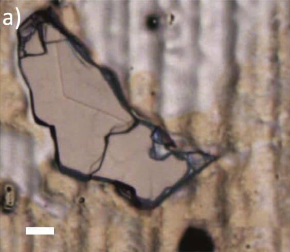
First what is the benefit of growing graphene on hexagonal boron nitride?
Once you can encapsulate graphene in hexagonal boron nitride – which is also atomically thin layers – you have a perfect way to protect the graphene’s quality. It is a dielectric material so if we deposit it on the right surface it also allows deposition of flatter graphene.
So it’s a very interesting combination for a lot applications in electronic devices. Beyond the fact that the association of these materials displays other interesting properties, one of the big challenges is large-scale growth of both together by CVD [chemical vapour deposition]. This work is reporting a very interesting methodology in order to get simultaneous large-scale growth of hexagonal boron nitride and graphene altogether in the same experimental process.
So could this enable large-scale use?
Exactly – all the beauty of graphene is in terms of physics, and its use for applications is related to the high quality of the material. Most of the devices that have been investigated so far having this high quality have been fabricated by so-called mechanical exfoliation: so you start with the graphite and exfoliate one layer of graphene and then do the same with a high-quality hexagonal boron nitride crystal. But in the process of transferring the layers you accumulate a huge number of defects because it is not easy.
On the contrary, with CVD growth you have all the gases and materials in the same experimental set up, and so you would grow first in this case boron nitride and then grow the graphene on top. You don’t change the atmosphere, you don’t change the condition, and you don’t transfer, so you reduce the density of defects and this is really nice. And actually in this paper they characterize the resulting carrier mobility for instance and they got really encouraging results. This challenge they have tackled is one of the most important challenges today for graphene and 2D materials research, so I’m really happy to have this paper in the issue.
Ultra-long wavelength Dirac plasmons in graphene capacitors Graef H et al. 2018 Journal of Physics: Material 1 01LT02
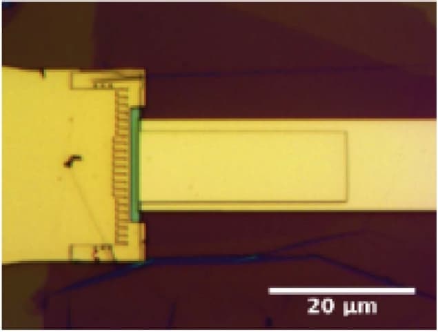
What makes plasmons particularly interesting in graphene?
When you shine light on the surface of metallic materials you excite collective modes of vibrations of the electrons, and so you transfer the information you are conveying with light onto the electrons – it’s a conversion of energy and information. Contrary to metals what we gain with graphene is we can tune the charge densities with an external electric field. So we can tune the properties of the plasmons that are created with light, which is something we couldn’t do with metals before. This additional tunability of the plasmons in graphene is unique.
People have been working on plasmons in graphene in quite a high energy range because they need to reach a certain quality in terms of the plasmonic resonance. The problem is this energy range makes for easy coupling between the graphene and substrate, so the plasmons then become coupled to other surface modes of the substrate – phonons and things like that – and this reduces their quality and lifetime etc.
So what has been achieved in this paper, by encapsulating graphene between two boron nitride layers they could achieve high-quality graphene where the graphene is disconnected from the substrate thanks to the boron nitride. So then they could have excitation of plasmons that are very weakly coupled to any other source, giving access to plasmon characteristics that were not within reach when we had just graphene on the substrate. (This device is made by exfoliation as mentioned before so it is not large-scale, just one device.)
So then we could have very complex plasmon-driven devices that could be much more efficient in, for example, detecting microwave vibration or for wireless communication or sensing. So this ultrasensitivity is opening up a new perspective in the field.
Do you see potential for developing this work by direct CVD as described by the previous authors?
Fantastic question, and actually this is what these two different groups of people should do! It is clearly a necessary step to bring a discovery or demonstration, a proof of concept to one device and then to upscale to see how the device will function at large scale, under conditions with more defects etc. But they can be grown at wafer scale. So if we want to integrate a lot of these plasmon-based electronic devices, we can have hundreds or thousands or millions of them on a chip.
So these two papers are very illustrative of the challenges of research in 2D materials – on the one side you have the forefront of research trying to really get high-quality research devices, and then trying to explore what is unique about these 2D materials, and to demonstrate that they can really bring high value in terms of applications. Then on the other side you have people making efforts to integrate these materials and to upscale their growth so that they can be practical for industries in the medium term.
Towards microscopic control of the magnetic exchange coupling at the surface of a topological insulator Ruβman P et al. 2018 Journal of Physics: Materials 1 015002

What makes topological materials so interesting?
These materials were predicted theoretically in 2005 – in fact in 2005 a lot of things happened, also the discovery of graphene – then it took a couple more years to have an experimental demonstration, proof that these materials actually existed and could be fabricated. Since then the field has been growing in terms of the community and the interest. What makes them so interesting is they provide a new dimension for surface states with certain spin properties that can be used in the world of spintronics.
These materials have a very high spin-orbit coupling and because of their inner symmetries and the spin-orbit coupling, they have a bulk bandgap – they are insulators – but conducting surface states. These conducting surface states are very robust to any imperfection at the surface, which is why you say they are protected by topology. This strong protection of surface states, where the bulk is insulating, is a unique property of this class of topological matter.
Beyond all the interesting properties that people have been looking at so far, one very exciting property is a new quantum phase called the quantum anomalous Hall effect. It has been proposed to use magnetic impurities so that these magnetic impurities can break the robustness of these surface states and reopen a gap. But then other states are formed at the boundaries of the surface, and those states are again topologically robust and convey a type of quantum Hall effect. And this is very interesting for the standardization of conductance – the material can serve as a standard of the conductance unit because those states convey a single quantum conductance channel. In addition these states can be used to encode information and to make a kind of intransitive sensor, and so on.
What have the researchers done in this piece of work?
It turns out that doping the surface with these magnetic impurities has been studied for a long time. But the result has been very controversial, and depending on the type of magnetic dopant – manganese, cobalt or iron – people were finding different results. In some cases it would open a gap and you get this quantum anomalous Hall effect, and in some cases it was not possible. So there was a need for a much more microscopic investigation of how a particular type of magnetic impurity segregates and interacts on the surface.
What we expected is that in order to have this gap opening and the formation of these additional bondless states, we need to have these magnetic impurities interact with each other and create a magnetic state at the surface, which would be a ferromagnetic state. So this cannot happen in any kind of condition it all depends on the type of magnetic impurity, on the type of topological insulator where you deposit these impurities, and also on the density, which determines whether they will segregate or not.
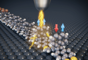
What is reported in this very interesting paper is microscopic studies of the interaction in two cases – manganese and cobalt. For the first time they can provide very valuable information about how these different types of magnetic impurities behave in terms of creating or not long-range ferromagnetic ordering, which will then drive the opening of a gap and the possible formation of this quantum anomalous Hall effect.
Where do you see the field going next – does this settle the controversy?
I think this really is a step forward – they really differentiate the manganese from cobalt with a total difference between between both types of magnetic impurities. But they also show that even if you take the one that can generate ferromagnetic ordering, you can tune these properties by changing the electronic density by doping, or by changing the concentration on the surface. So again this is the tunability that they investigated and reveal. And tunability is always interesting because then you can really have a recipe, which tells you not just how to generate a property, but also how to switch it on and off just by an external electric field, for example. So I think that is opening a new dimension of research in this field.
And the authors also mention that they are very interested in spin configurations named skyrmionic states, which is a very complicated spin texture of the magnetic impurity that has potential applications in next-generation memories or spintronic technologies. I think they are opening a window to search for more complicated magnetic states at the surface. So it really is a fantastic paper to have in our journal because they are clarifying some of the controversy, but also opening a new dimension for this type of research.
Flexible nanogap polymer light-emitting diodes fabricated via adhesion lithography (a-Lith) Wyatt-Moon G et al. 2018 Journal of Physics: Materials 1 01LT01

What do the researchers mean by adhesion lithography here?
This is a specific technique that they have developed to obtain very narrow nanoscale structures, to really start to embed nanopatterning in these organic light-emitting diodes (OLEDs). So this is really based on chemistry, and they contrast this chemistry with other types of technology that can go down to very short scales in terms of patterning.
The breakthrough and the idea is to really start to develop a generation of nanoscale light sources that can become mainstream in the next-generation of let’s say ultrahigh definition and small size displays. We see OLEDs are becoming mainstream in many applications including smartphone technologies. But having a nanoscale source of light is also very interesting in the world of biotechnology and biolelectronics, where the miniaturizaiton of the light source provides an interesting property to control certain kinds of reaction induced by light at the nanoscale.
So this paper is another interesting study where there is an advance in terms of fabrication and this advance in terms of fabrication is connected to characterization of the material that is produced and really shows the perspective in terms of application. So this is again a very timely illustration of what the Journal of Physics: Materials aims to become, aims to be – that is, showing the community where we are going today in terms of the forefront of materials, and what is the prospective landscape in terms of applications.
What can they do with adhesion lithography that they couldn’t do before?
The main point is to bring metallic electrodes very very close together, with an interelectrode distance of just a few nanometres or 10 nm at most, but also to have a very large control of the aspect ratio of the electrode geometries. Then the organic material is deposited on top and bridges the gap to emit light so they have a green-light-emitting OLED. This type of lithography gives variability and versatility in terms of controlling the aspect ratio of the different materials in place, allows them then to have a versatile platform that will adapt to the needs of the application – type of light to be emitted, the dimension and so forth, and the architecture and integration of the light source on the same substrate.
Also of interest to me, they develop a technology that can be embedded on glass or plastic substrates. So this becomes a low-cost technology, and this is a very important part of the work. If you base your technology on silicon only and you want to go to miniaturization the cost is increasing higher and higher as you narrow down the size of the device. In this case glass and plastics are very common materials, the cost is very low and their technology is chemically driven so it doesn’t really add an additional cost. Instead it brings versatility, complexity in terms of the possible architectures, and it brings a light source at the nanoscale – that’s a new dimension for a lot of applications.
Suppose there were a worldwide apocalypse that would swallow up all scientific knowledge in one gulp and you could save one of these papers, which would it be?
That is a tremendously complicated question! You know I don’t think one paper will save the whole of humanity. All the papers we have been talking about today are really papers that are positioned at the forefront of peer-reviewed research and the developments of material science and technology. My guess is those papers will serve in the next years and probably decades to come in providing society with technology that is much more energy efficient. This is really one of the main challenges that we are facing today because the waste of energy in current technology is too high, and consumption is too high. Materials with improved performance means the cost in terms of energy consumption will be reduced, and this is very important for the challenge that society faces today. So maybe I would say if you have to choose one journal, maybe Journal of Physics: Materials would be one of the best to keep.
What attracted you about this journal to take on the role of editor in chief?
I accepted the offer to join as editor in chief because I was really convinced that this journal had a place to occupy – a territory to propose for various communities that was not really available elsewhere. We have to say that there are many many journals – actually the emergence of new journals is a bit impressive and overwhelming – and we see that the journals are focusing more and more on a narrower scope. Journal of Physics: Materials on the contrary wants to emphasise the quality of the science but wants to keep a large landscape so that we have a platform where advances in novel materials or the foundation for technologies will knit together and inspire other authors publishing in the journal to collaborate – as we may have with the two groups publishing on graphene related research. So that’s what we expect, and that’s why I think the journal is really bringing new value for a scientific publication, and this is why I decided to join.
I’m very happy to be so supported by IOP and the publisher of Journal of Physics: Materials. Things have been very smooth and this first issue is a great encouragement for us to proceed. We also selected a senior advisory panel and we have an editorial board, and our success is mostly due to the large contribution and excitement of many of the members of these communities. It’s not so easy – when you launch a new journal you don’t have a clear position in the landscape and you don’t have an impact factor so it’s not so straight forward for people submitting their paper because there is no impact factor and the paper cannot be tracked for a year or two. Having so many colleagues in so many different fields of materials science so enthusiastic has been a great support and encouragement for me. I think we have a very good expectation of the journal because most of our colleagues are very proactive, we have a lot of focus issues in the pipeline and another issue coming soon – they are completely driven by suggestions of editorial board members or members of the advisory panel. And it’s unbelievable how motivated most of them are and that’s a great sign for the journal to become one of the standard bearers in the years to come.

