Atomic force microscopy can successfully be used to distinguish between different atoms in doped graphene nanoribbons, according to new measurements by researchers in Japan, Finland and Switzerland. The technique, which works by quantifying the differences in the van der Waals radii of the atoms, could be used as a general way to analyse technologically important functionalized 2D carbon materials.
Among 2D materials, graphene (which is a flat sheet of carbon just one atom thick) is one of the most attractive for a host of device applications thanks to its unique electronic and mechanical properties. Indeed, graphene has even been touted as being one of the best alternatives to silicon as the electronic material of choice in the future.
However, unlike the semiconductor silicon, there is a big problem in that graphene has no gap between its valence and conduction bands. Such a bandgap is essential for electronics applications because it allows a material to switch the flow of electrons on and off.
Introducing a bandgap
One way of introducing a bandgap into graphene is to make extremely narrow ribbons of the material. What is more, if heteroatoms are incorporated into a precursor when synthesizing graphene, doped graphene nanoribbons (GNRs) can be produced. The position and density of the doping elements can be controlled in these ribbons, which, in turn, allows the electronic properties of the ribbons themselves to be controlled on the atomic level.
Researchers have so far succeeded in substituting single heteroatoms of nitrogen, boron, sulphur and oxygen into GNRs. Until now, however, they have not really looked at chemically analysing these atoms and characterizing how they substitute for carbon atoms in the graphene lattice.
Discriminating between boron, carbon and nitrogen atoms
Adam Foster of Aalto University in Finland and colleagues have now used the CO-functionalized tip of an atomic force microscope (AFM) to discriminate between boron (B), carbon (C) and nitrogen (N) atoms embedded at the centre of a GNR thanks to the differences in their van der Waals radii. They were also able to measure the modulated electron density caused by the substitution.
The researchers embedded heteroatoms at equivalent atomic sites in the nanographene ribbons using in-surface chemical reactions with special precursor molecules. Similar to previous work they had done on periodic boron-doping into GNRs, they used C4BN cyclic rings to provide the boron and nitrogen atoms. They annealed these compounds with the GNRs at 200°C and then at 400°C to induce cyclohydrogenation and form BN-GNRs.
Resolving the inner structures of BN-GNRs
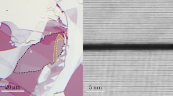
Atomic force microscopy is a widely-used ultrahigh-resolution technique that allows researchers to observe extremely small objects, even down to single atoms. It works by sensing the topography of a sample as it scans across it thanks to a very fine probe (the cantilever), which has an extremely sharp tip at its end that touches the surface of the sample. In this work, Foster and colleagues succeeded in resolving the inner structures of the BN-GNRs and found that a nitrogen site, for example, appears as a dark site. An adjacent bright site corresponds to a boron atom.
Thy obtained their results by taking a series of AFM images at different heights. When the tip and sample are well separated from each other, weak and bright contrast appears at the boron site but as the tip is moved closer to the BN-GNR, the researchers are able to distinguish six-membered carbon rings. And at a height of 32 picometres, three C-N bonds also appear. Since the CO-tip AFM is subject to short-range repulsive interactions, the contrast in the images shows that the onset of short-range repulsion occurs first at B sites, then at C sites and finally at N ones.
“In this work, we focused on discriminating between different heteroatoms, but this GNR is a very exciting material in its own right,” says team member and lead author of this study Shigeki Kawai of the National Institute for Materials Science in Tsukuba in Japan. “We would now therefore like to investigate its electronic properties in detail as well as make devices from it and study these too,” he tells nanotechweb.org. Kawai did the experiments for the present work, which is detailed in Science Advances DOI: 10.1126/sciadv.aar7181, while he was at the University of Basel in Switzerland.