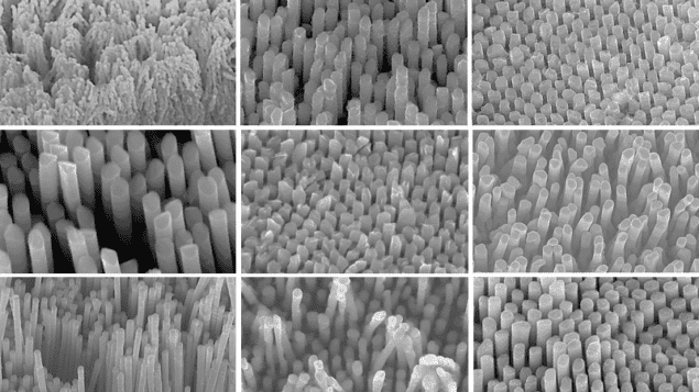
Researchers in the US and China have shown that diffusion at the atomic scale enables long nanowires of crystalline metals to be fabricated using a single-step moulding technique. The nanomoulding method is much easier and more cost-effective than current fabrication techniques, which could open up new applications for metallic nanowires. What’s more, unlike with other fabrication techniques, narrower nanowires are easier to produce than those with larger diameters.
Moulding is a common fabrication technique in which a malleable material is formed into a 3D structure by forcing it into a pre-defined template. For nanoscale features, however, this method is limited by the size of the so-called “flow unit”. In polymers, for example, the flow unit is a molecule – typically about a nanometre in size – which makes them suitable for nanomoulding. But this technique has not been considered a viable option for metallic materials, since in this case the flow unit is a grain – which is much larger. This has required the use of more costly methods, such as lithography, to etch nanopatterns onto crystalline metals.
So it was a surprise in 2017 when Ze Liu of Wuhan University in China showed that crystalline metals can be moulded into high-aspect ratio nanowires at temperatures below their melting point. While this low-cost, one-step fabrication method is clearly advantageous, Liu could not explain the mechanisms behind this unexpected finding.
More recently Liu teamed up with researchers from Yale University in the US to investigate the method further. Experiments revealed, somewhat counter-intuitively, that it was easier to produce nanowires with smaller radii using the nanomoulding technique. When fabricating the wires for the same amount of time, narrow nanopillars were significantly longer than those with larger diameters. This was unexpected, since capillary forces and the size of the flow unit should make moulding more difficult at smaller scales.
Since the mould cavities are smaller than a metal’s grain, the researchers knew that most deformation mechanisms could not be responsible for creating the nanowire structures. Instead, they concluded that atomic-level diffusion is the main process that drives crystalline metal nanomoulding.
According to the research team, the pressure applied to the metal during nanomoulding generates a concentration of vacant-atom impurities. These vacancies allow metallic atoms to propagate through the mould cavities, a process that they confirm can explain their curious observations of increasing the wire length for smaller radii.
Jan Schroers from Yale, a member of the research team, shares his surprise at the discovery that “atomic diffusion is capable, atom by atom, to produce these very long nanowires”. As the properties of metal nanostructures strongly depend on their sizes and shapes, this quick and easy method is bound to find wide application. “Nanotechnology needs a technique that can fabricate a much broader range of materials on the nanoscale,” Schroers comments. The researcher suggests that advanced fields such as biosensing and catalysis are likely to benefit the most from this discovery in the short term, but he also sees future use in quantum devices. As a next step, the team plans to see whether this diffusive nanomoulding can be used to form intermetallic phases.
Full results are published in Physical Review Letters.


