An international group of researchers has shown that electrons can travel more than 10 μm in graphene nanoribbons without scattering – which is much further than predicted by theory. Even more surprising, the team spotted a large jump in the electrical resistance of sections of nanoribbon that are longer than about 16 μm. These puzzling results could suggest that graphene harbours a new type of electronic transport mechanism hitherto unknown to physicists.
Graphene is a sheet of carbon just one atom thick that has shot to fame over the past decade after physicists worked out how to create freestanding flakes of the material. It is a semimetal that is an extremely good conductor of electricity because its electrons can travel very close to the speed of light. However, the presence of imperfections and impurities mean that an electron can travel only about 10 nm in a freestanding flake of graphene before scattering, which increases the electrical resistance of the material.
A promising way forward is to make devices using epitaxial graphene, which is a single layer of carbon grown on a substrate such as silicon carbide. As well as being amenable to commercial fabrication techniques, devices based on epitaxial graphene can be made with great precision and with small numbers of impurities and imperfections.
Ballistic electrons
Now, Walt de Heer and colleagues at the Georgia Institute of Technology – along with researchers in Germany, France and the US – have created pristine ribbons of epitaxial graphene just 40 nm wide. They have shown that electrons can travel along the edge of the ribbon without scattering. This behaviour is much like photons travelling along an optical fibre, or bullets fired from a gun – which is why the electrons are called “ballistic”.
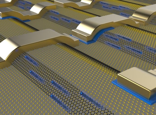
The nanoribbons were created on a silicon-carbide wafer in a process that involves creating trenches in the wafers and then heating the wafer to a temperature of more than 1000 °C. This causes silicon atoms near the surface to evaporate and carbon atoms to migrate to the sloped walls of the trenches, where they form nanoribbons along the lengths of the trenches (see figure).
Bumping into the probe
Ballistic transport was confirmed by studying the electrical properties of the nanoribbons using a traditional four-probe measuring scheme. When a probe is attached to a nanoribbon, the ballistic electrons bump into it, which results in a huge increase in the electrical resistance of the nanoribbon. By contrast, a collision with the probe by a conventional conduction electron has a minimal effect on the resistance because these electrons will have already undergone many collisions as they travel along the nanoribbon. When a second probe is placed on the nanoribbons, the resistance increases dramatically again, thus confirming that the current flowing through the nanoribbon is being carried by ballistic electrons.
An important parameter describing ballistic transport is the average distance an electron travels before it collides with the atoms in a nanoribbon. Ballistic electrons encounter very little electrical resistance; but as soon as they scatter, the resistance increases. The team determined the “mean free path” travelled before a collision by measuring the increase in resistance of sections of a nanoribbon that varied in length from 1–5 μm.
Big surprise
This study revealed a small change in resistance over the distances studied and this allowed the team to extrapolate a mean free path of about 100 μm. However, when the researchers measured resistances over longer distances, they got a big surprise. At distances greater than 16 μm the resistance increased rapidly with length and it became clear that the mean free path was much shorter than the extrapolated value.
While the reason for this rapid increase remains a mystery, De Heer speculates that it could have something to do with the fundamental nature of the ballistic charge carriers. Instead of being elementary particles, he believes that the charge carriers could be quasiparticles – particle-like entities that arise out of interactions between electrons and the surrounding graphene lattice. A classic example is the Cooper pair of electrons that transports charge in some superconductors. De Heer suggests that charge-carrying quasiparticles in graphene could have a finite lifetime, which only allows them to travel about 16 μm in a nanoribbon before they decay.
The idea that new physics could be lurking in graphene is also backed up by the fact that the measured resistance of the team’s nanoribbons is much lower than that predicted by theory.
The next step for the researchers is to try to gain a better understanding of exactly how charge is carried in graphene. The team has already made a nanoribbon in which the current is split along two paths before being recombined. By studying the quantum interference that occurs in such devices, the researchers hope to determine important properties of the charge carriers and work out if these are indeed quasiparticles.
The research is described in Nature.


