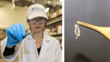
A camera made by combining graphene with industrial semiconductor processing has been unveiled by researchers in Spain. Their device is sensitive to a wider spectrum of light than any commercial camera and the team says that the new process could also be used to create high-speed optical interconnects for communications networks.
Graphene is a sheet of carbon just one atom thick and this “wonder material” has a number of very useful electronic properties, such as an extraordinarily high electron mobility. As a result it has been used to create displays, loudspeakers, touchscreens and other electronic devices. However, most of these applications are in the early stages of development and researchers and companies are still working on how to integrate graphene into industrial-scale manufacturing processes.
Today’s electronics industry is dominated by the complementary metal-oxide semiconductor (CMOS) process, which combines silicon with metals and insulators on single wafers that can contain billions of transistors. Integration of other semiconductors such as graphene into CMOS, however, poses a problem because the lattice mismatch between different materials usually makes it impossible to grow high-quality layers of other semiconductors on silicon. Indeed, when graphene electronic devices have been created, they have not been integrated into CMOS circuits.
Limited range
The inability to integrate other semiconductors puts restrictions on the performance of CMOS-based cameras. “The camera in your smartphone can only see visible light as silicon only absorbs visible light,” explains Frank Koppens of the Institute of Photonic Sciences in Barcelona. “If you want to detect infrared light you have to buy an indium gallium arsenide camera, for example. That will cost you around $40,000 or $50,000 because indium gallium arsenide is not monolithically integrated with CMOS, so they have a very complicated process to integrate the readout circuit with the photodetectors.”
In 2011, Koppens and colleagues produced a high-sensitivity photodetector for both infrared and visible wavelengths by attaching two electrodes to a sheet of graphene covered with lead sulphide quantum dots. Photons absorbed in the quantum dots create electron-hole pairs. The electrons were retained in the quantum dots, while the holes moved down into the graphene, dramatically increasing its electrical conductivity and producing a large increase in current. However, the researchers could not then go on to produce a camera. “A photodetector you can just wire up to an electronic board,” explains Koppens. “A camera needs to read out one million photodetectors at the same time, so you need a micro-electronic circuit.”
In the new work, Koppens’ team transferred graphene epitaxially grown on copper foil onto the surface of a silicon CMOS chip. The chip was embedded with the circuitry to read out each camera pixel individually. They then patterned the graphene to define each pixel and deposited a layer of quantum dots on top. The resulting camera can detect wavelengths from 300 nm (near-ultraviolet) to 2000 nm (short-wave infrared). Even though the graphene is not used to absorb the light, its extraordinarily high electronic mobility produces a stronger signal, which allows it to detect infrared light above noise where other devices cannot. The researchers believe the device could find use in cameras for smartphones, security systems, vehicles, and food and pharmaceutical inspection systems. Crucially, its integrated CMOS production could make it no more expensive than current smartphone cameras.
Unprecedented speeds
The researchers are also working to produce graphene-based optical interconnects, which could boost the capacity of optical communications networks and even lead to optical computers. Although, in the current design, the quantum dots limit the speed of the camera, graphene itself can absorb light – albeit much less effectively – at unprecedented speeds: “For data communications you need to integrate graphene with silicon photonics,” says Koppens. “That’s also a silicon CMOS-based technology.”
Andrea Ferrari of the University of Cambridge in the UK told Physics World, “The most important result [of the research] without any doubt is the first bona fide, large area graphene-CMOS integrated device”. Ferrari, who was not involved in the research, adds: “This is the last challenge when it comes to graphene optoelectronics.” He says one of the next big hurdles will be to develop a production process suitable for “fabs” – the billion-dollar production facilities that produce commercial CMOS chips. “If graphene-CMOS integration actually works properly in the fab, then we are done: we are looking at a major revolution, with optoelectronic devices in your phone, in data transmitter units for the internet of things – all based on graphene,” he says. “This is a major result”
The research is described in Nature Photonics.


