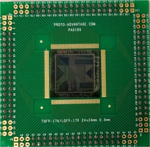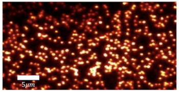
As space missions venture ever further afield, spacecraft will inevitably be exposed to greater amounts of cosmic radiation that can damage or even destroy their onboard electronics. Researchers at the Massachusetts Institute of Technology (MIT) and the US Air Force Research Laboratories have now shown that adding carbon nanotubes to transistors and circuits could render these devices resistant to higher amounts of radiation than is possible with standard silicon-based electronics.
Cosmic radiation is ionizing radiation made up of a mixture of heavy ions and cosmic rays (high-energy protons, electron and atomic nuclei). The Earth’s magnetic field protects us from 99.9% of this radiation, while the remaining 0.1% is significantly attenuated by our atmosphere.
Electronics designed for space applications have no such protection, however, and researchers are investigating ways of using emerging nanomaterials to mitigate the problem. Carbon nanotubes (CNTs), which are rolled-up sheets of carbon just one atom thick, are one promising possibility. These materials are beginning to be employed in electronics components such as transistors because they are more energy efficient than standard silicon-based devices. The radiation toleration of carbon-nanotube-containing field-effect transistors has not, however, been widely studied until now.
Electrical properties protected
In their work, a team led by Pritpal Kanhaiya and Max Shulaker deposited CNTs on a silicon wafer as the semiconducting layer in field-effect transistors (FETs). They then added radiation shields consisting of hafnium oxide, titanium and platinum to the semiconducting layer. They found that placing the shields both above and below the CNTs protected the electrical properties of the FETs against incoming X-ray radiation up to a dose of 10 Mrad (107rad). When a shield was placed only beneath the CNTs, they tolerated doses of up to 2 Mrad, which is similar to commercial silicon-based radiation-tolerant devices.
Protecting self-driving cars from cosmic rays, size limits for wind farms
The researchers say their CNT-containing FETs, which they describe in ACS Nano, owe their high radiation tolerance to both extrinsic and intrinsic properties. The former include the fact that the devices can be fabricated at temperatures below 400°C. This makes it possible to engineer the device in geometries that are more tolerant to “total ionizing dose” effects – that is, to long-term ionizing damage. Intrinsic properties include material properties of the CNTs themselves, which provide radiation tolerance for so-called transient upsets that occur when ionizing radiation strikes the semiconducting channel in a device. The energy produced by the ionizing strike generates large amounts of electrons and holes within the semiconductor, creating charge disturbances and temporary current fluctuations.


