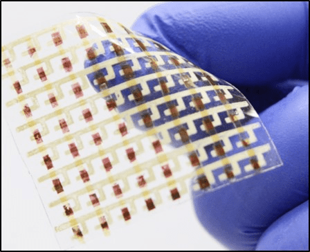
A stretchable, high-performance semiconductor device with fully integrated electronics and logic circuits has been created by Cunjiang Yu and colleagues at the University of Houston. Their low-cost semiconductor material retained its high charge carrier mobility, even when subjected to 50% stretching. The team’s work could lead to the development of practical new technologies including robotic skins and wearable electronics.
Researchers around the world are trying to develop electronic devices that can stretch and then return to their original shape. If realized, stretchable semiconductors could have a diverse range of potential applications including robotics, bioelectronics, and medicine.
So far, efforts to create commercially-viable stretchable electronics and logic circuits have included semiconductors with intricate microscopic structures that allow them to stretch on macroscopic scales; taking the form of either foldable molecular concertinas, or rigid islands connected by stretchable links. Yet these structures are expensive to create, and would be difficult to manufacture on large scales.
Alternatively, recent research has seen progress towards stretchable, rubbery semiconductors made from polymer nanofibers percolated in a silicone matrix. These materials have a far more scalable manufacturing process, but because of their polymer structures, they are currently hindered by a low charge carrier mobility. This occurs because electrons must travel over large distances in such materials, meaning they cannot carry charge quickly enough to be commercially competitive.
Carbon fascination endures in nanoscience
Conducting highways
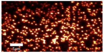
In their study, the Houston physicists aimed to fabricate an intrinsically stretchable rubbery semiconductor with both a high carrier mobility and a low-cost, scalable manufacturing process. To do this, the team introduced metallic carbon nanotubes as dopants on the surface of a rubbery semiconductor composite. The nanotubes provided a network of conducting “highways” across the material, greatly reducing distances over which electrons need to travel; therefore, improving their semiconductor’s carrier mobility.
Yu’s team then integrated circuits of transistors into their doped semiconductor, allowing them to demonstrate fully-integrated logic gates and electronics. In addition, the researchers demonstrated its performance as a sensitive, elastic skin which can map physical touch. During these tests, the material retained its electrical performance even with 50% stretching, with little substantial loss in carrier mobility.
The team’s results show promise for future developments of applications including robotic skins which are sensitive to touch, implantable bioelectronics for use in medicine, and improved interfaces between humans and machines. In the future, Yu and colleagues hope to improve carrier mobility even further, allowing them to build yet more complex digital circuits.
The new material is described in Science Advances.


