As the International Year of the Periodic Table launched in Paris, France, last week, a celebration of the technology enabled by advances in nanoscience drew crowds to the Big Sight conference centre in Tokyo, Japan. Investigations of features at the nanoscale have brought new properties and behaviour to light for a number of elemental groups and classes, but the element with an incomparable track record of ceaseless reinventions is carbon.
Carbon future tech
As the element underpinning the whole of organic chemistry carbon never had humble claims. Exhibits and sessions at Nanotech 2019 spoke volumes about how research and development to exploit the flexibility, versatility and often cheaper processing of organic compounds is booming. Representatives at Kyushu University described how chemically engineered polymers were bringing solutions to organic LEDs and potentially organic lasing. While at a materials informatics session researchers from the National Institute of Advanced Industrial Science and Technology (AIST), Tohoku University, the Institute of Statistical Mathematics, Research Organization of Information and Systems, and Mitsubishi Chemical Corporation described algorithms for both large virtual chemical database machine learning and small database “transfer learning” to unearth polymer designs with desired property combinations.
The absence of prominent nanoscale features in many of the displays at Nanotech 2019 speaks volumes of how the term “Nanotech” is increasingly used more figuratively as synonymous with “next-generation technology”. The exhibit abounded with impressive demos, and from the company Carbon’s 3D printed trainers in collaboration with Adidas to the lignin based cars by the research consortium behind (SIP-Lignin), carbon played a role in many of the materials featured.

Carbon in zero to three dimensions
At the other side of Big Sight in the 1&2DM conference the role of nanoscale features was very much in the foreground. As the homeland of Sumio Iijima – the scientist who discovered carbon nanotubes (CNTs) in 1990, and who also opened the conference plenaries – Japan has cherished a strong government-funded research landscape in these one-dimensional rolls of honeycomb-shaped carbon lattice. Although preceded by the 1985 discovery of buckminster fullerene – football-shaped structures of carbon – the impressive electronic and mechanical properties of CNTs really catapulted nanocarbons into the eye of industry. Mauricio Terrones at Japan’s Shinshu University and the Pennsylvania State University in the US highlighted how their biocompatibility has also opened up opportunities for exploiting them in medical applications, such as viral filters for diagnosis.
Since the 2005 isolation of graphene – dubbed the “wonder material” for its array of electronic, optoelectronic and mechanical properties – interest in 2D materials surged. However, what the closing plenaries at 1&2DM emphasised most was the developments taking place in multidimensional nanosystems.
Can 2D materials contribute to consumer electronics?
Graphene is no stranger to industry and Byung-Hee Hong, at Seoul National University and Graphene Square, South Korea, and Stephan Roche at ICREA and ICN2 in Spain led attendees through some of the advantages the materials has offered for applications from mobile phones to treatments for Parkinson’s disease and osteoporosis. Improvements in fabrication mean that companies like Air Membrane (a spin out from Masatoshi Hasegawa’s group at AIST) are now able to offer production of electronic grade graphene, which has higher crystal quality requirements, at scales that are relevant to industry. But as Nobel laureate Kostya Novoselov told attendees as he described the moment when he and fellow laureate Andre Geim at Manchester University in the UK first isolated graphene, “The next important step was when we realized we could go from 2D back to 3D.” He went on to describe the tunable band electronic structures and tunnelling magnetic properties in 2D material superlattices, as well as recent work synthesizing zero-dimensional graphene dots in 2D hexagonal boron nitride (hBN), which might then be layered in a 3D superlattice. Stephan Roche later described the work as, “A new playground now – it’s beautiful.”
The next important step was when we realized we could go from 2D back to 3D
While a lot of research in 2D materials focuses on producing pristine crystals or crystals with regular defects to access their extraordinary properties, Barbaros Oezyilmaz at the National University of Singapore showed how amorphous 2D carbon structures with random bond lengths and angles also have interesting traits to explore. A researcher who works particularly closely with industry, Oezyilmaz told attendees, “Interacting with companies helps us define what we need but also pushes us in new research directions,” adding that the right collaboration is key. Perhaps as a result he was quick to pinpoint potential applications of amorphous 2D carbon such as exploiting their low-k dielectric properties in electronics, their chemical inertness in anti-oxidation coatings or their use in battery electrodes.
Efforts to exploit graphene in electronics has led to extensive research over the past 15 years into producing nanoribbons where the finite width gives rise to a bandgap, an electronic property the semiconductor industry hinges on. Most protocols for nanoribbon synthesis either unzip carbon nanotubes or cut graphene into strips, that is, moving from 2D towards 1D. Akimitsu Narita at the Max Planck Institute for Polymer Research, Germany, described a purely bottom up chemical approach that allows unprecedented control over parameters such as chirality and edge states, including armchair and zig zag shaped edges as well as coves and other edge features. The deft chemical manipulation of the nanoribbon parameters makes it possible to explore a rich range of properties including some of the exotic topological states described in the subsequent plenary by Katsunori Wakabayashi at Kwansei Gakuin University, Japan.
Holey nanocarbon
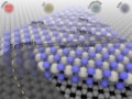
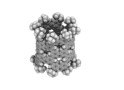
On the other side of Tokyo at Tokyo University Hiroyuki Isobe and his team are also pushing the boundaries of carbon chemistry control. The new chemistry lab is kitted out with an appreciation of convenience as well as state of the art, including features unique to fault-line research bases, such as a chemical bench attached to both ceiling and floor for earthquake resilience, as well as 360 degree lighting to minimize shadows for a clearer view while handling chemicals. Here Isobe and his team developed the chemical procedures to synthesize and join rings of phenine molecules to produce precisely defined phenine nanotubes – a reinvention of the carbon nanotube where phenine rings of carbon atoms replace each carbon atom.
“Carbon nanotubes are one species, but as chemists we consider each sample a collection of several molecular entities because the length and so on are not defined,” he tells Physics World as he explains the difference in precision synthesis between conventional CNT growth and the work in his lab.
The phenine ring structures have already revealed a number of surprises. Isobe and his team showed they could trap a Buckminster fullerene in the ring and what is more, the ball would spin in an inertial mode as temperature increases. Much remains unanswered but the researchers believe the unidirectional motion could arise from the difference in energy for forward versus backward motion due to the chirality of the ring. The apparently ordered motion from heat energy input may at first raise alarms concerning the second Law of Thermodynamics, which states that the entropy of a system should always increase, but taking a system of multiple ring entrapped fullerene balls at random orientations as a whole may settle these qualms.
New nanocarbon hits the scene
While fascinating from a fundamental science point of view, applications of these molecular motors remain remote. However, the optoelectronic properties may be easier to harness. Isobe describes how the direction of electron flow round the molecular cylinders cancels at adjacent rings in the direction perpendicular to the ring plane, so that the sum current is parallel to an applied magnetic field. This leads to interesting effects for holograms, which rely on the chirality of emitted light where the figure of merit, the g factor, is proportional to the cosine of the angle between field and current. Where the field and current are parallel this cosine reaches its maximum of one so that the g factor of these molecules is around 0.15, more than 10 times that of any other organic molecule.
There was a time when pure carbon was essentially either soot, pencil lead or diamond. With advances in nanoscience these dichotomies have bred and multiplied so that the permutations of possible carbon structures seem endless. And with each additional product successfully synthesized a whole new catalogue of properties and potential avenues for developments in both fundamental and applied science emerges, so that the fascinating partnership of nano and carbon science seems likely to endure for many years to come.
- edited 21 Feb 2019