Nitrogen-vacancy (NV) impurities in diamond have optical and electronic properties that make them ideal for developing quantum technologies, including quantum computers and quantum sensors. However, creating NVs with nanoscale precision has proven difficult and a barrier to making practical devices. Now, physicists in the US and Australia have developed a new technique for making NV centres at precise locations within tiny, high-quality optical cavities.
Atomic impurities, or defects, in natural diamond give rise to the pink, blue and yellow hues often seen in the precious stones. One such defect involves two adjacent carbon atoms in the diamond lattice being replaced by a nitrogen atom and an empty lattice site (or vacancy). When illuminated with laser light of a certain colour, the NV centre emits light of another colour. The intensity of this light depends on the spin of the electron in the NV. An important property of the NV centre is that the spin is shielded from the surrounding environment and can therefore be used to store and process quantum information.
A challenge facing quantum-device developers is how to get light into and out of the NV in an efficient way. This could be solved by coupling the NV to an optical cavity, but conventional methods for creating NVs – such as ion implantation – are not accurate enough.
Atom-scale positioning
“To benefit from the enhanced emission made possible by optical cavities, NVs need to be positioned at a particular spot inside these cavities so that the two structures optimally interact,” explains team leader Evelyn Hu of Harvard University. “The problem is that cavities that are ‘matched’ to NV centres are challenging to fabricate. The NV centre is atom-sized, and thus understanding how to place it within exactly the right place in the cavity is difficult too.”
Using NVs grown by a technique called “delta doping” might be a solution to this problem, she says, because it allows us to position an NV in a cavity with unprecedented accuracy in the horizontal plane. “The term ‘delta-doped’ comes from mathematics – the ‘delta function’ – and in this case indicates that the NVs are intentionally created only within a 2D plane, and should not exist elsewhere,” explains Hu.
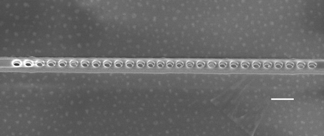
The cavity used by the team is called a “photonic crystal nanobeam” and is made by drilling a line of equally spaced holes (each about 150 nm diameter) in diamond. The cavity supports standing electromagnetic waves, and is designed to resonate at the frequency of the light emitted by an NV, thereby enhancing the light output of the NV.
Centring NVs inside a nanobeam
The researchers achieved their accurate positioning by first identifying the horizontal plane in which the NVs are located. “We are able to identify the z co-ordinates of delta-doped NVs – that is, we are able to work out the plane in which all of the NVs in a sample are located,” says Hu. “By forming the nanobeams around this plane, we are sure that all of the NVs are centrally located inside it.”
“Our cavities are also very high quality, which means that optical losses are kept to a minimum,” Hu says. “Indeed, we measured quality factors (Q) as high as 24,000. Previous experiments reported values of up to 6000.”
The team, which includes scientists from the University of California at Santa Barbara, the University of Chicago and the University of Technology in Sydney, says that it would now like to be able to accurately position the NVs in 3D – that is, within each horizontal plane.
The work is described in Applied Physics Letters.
- This article first appeared on nanotechweb.org


