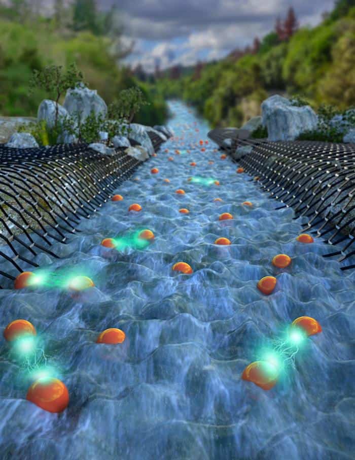
Electrons can behave like a viscous liquid as they travel through a conducting material, producing a spatial pattern that resembles water flowing through a pipe. So say researchers in Israel and the UK who have succeeded in imaging this hydrodynamic flow pattern for the first time using a novel scanning probe technique. The result will aid developers of future electronic devices, especially those based on 2D materials like graphene in which electron hydrodynamics is important.
We are all familiar with the distinctive patterns formed by water flowing in a river or stream. When the water encounters an obstacle – such as the river bank or a boat – the patterns change. The same should hold true for electron flow in a solid if the interactions between electrons are strong. This rarely occurs under normal conditions, however, since electrons tend to collide with defects and impurities in the material they travel through, rather than with each other.
Making electrons hydrodynamic
Conversely, if a material is made very clean and cooled to low temperatures, it follows that electrons should travel across it unperturbed until they collide with its edges and walls. The resulting ballistic transport allows electrons to flow with a uniform current distribution because they move at the same rate near the walls as at the centre of the material.
If the temperature of this material is then increased, the electrons can begin to interact. In principle, they will then scatter off each other more frequently than they collide with the walls. In this highly interacting, hydrodynamic regime, the electrons should flow faster near the centre of a channel and slower near its walls – the same way that water behaves when it flows through a pipe.
Extremely clean 2D materials
In recent years, researchers have created extremely clean samples from 2D materials such as graphene to act as testbeds for studying electron hydrodynamics. The vast majority of this work, however, involved measuring electron transport, which only probes the physics of electrons at fixed positions along the perimeter of the device.
“Hydrodynamics, on the other hand, brings to mind dynamic images of electrons swirling around with interesting spatial patterns,” says Joseph Sulpizio, who is one of the lead authors of this new study. “Such patterns have been predicted in theory but never imaged spatially.”
Poiseuille current profile
Sulpizio and the other researchers, led Shahal Ilani at Israel’s Weizmann Institute for Science in collaboration with Andre Geim’s group at Manchester University, have now imaged the most fundamental spatial pattern of hydrodynamic electron flow for the first time. They obtained this parabolic or Poiseuille current profile by studying electrons travelling through a conducting graphene channel sandwiched between two hexagonal boron nitride layers equipped with electrical contacts.
Under an applied electric field, the electrons produce a voltage gradient along the current flow direction. Unfortunately, this local voltage gradient is the same for both hydrodynamic and ballistic electron flow and so cannot be used to distinguish between the two regimes. Ilani and colleagues overcame this problem by applying a weak magnetic field to the sample, which produces another voltage – the Hall voltage – perpendicular to the direction of the current. The gradient of this voltage is very different for hydrodynamic and ballistic flow.
The researchers imaged the Hall voltage profile for both flow regimes using a scanning probe recently developed in their laboratory. This ultraclean carbon nanotube single-electron-transistor-based device is held at cryogenic temperatures and is extremely sensitive to local electrostatic fields. The current flowing through it is thus indicative of the local potential of the sample and voltage gradients associated with the Hall voltage.
By measuring this current, the team was also able to observe the transition between the regime in which electron-electron scattering dominates and that in which the electrons flow ballistically. “As expected, we observed a flat Hall field profile across the graphene channels at low temperatures,” Sulpizio tells Physics World. “Upon heating, however, the profile becomes strongly parabolic, revealing less current flow near the walls and more near the centre, which indicates the transition to hydrodynamic/Poiseuille flow.”
Magic-angle graphene reveals a host of new states
Implications for device development
The implications of the work, which has been published in Nature, are many, he says. Electron hydrodynamics only emerges at elevated temperatures (in contrast to many other kinds of electronic phenomena that exist only at very low temperatures) and this will be relevant for technological devices like computer chips that operate at room temperature. It will also be relevant in 2D van der Waals heterostructures like those made from graphene, and especially when they are super-clean. This behaviour is likely to play an important role in new generations of devices made from these materials.
“Looking further ahead, it might even be possible one day to engineer fundamentally new kinds of electronic devices that directly exploit electron hydrodynamics,” Sulpizio says. “When electrons interact hydrodynamically, their viscosity results in highly non-local spatial flow patterns that might be technologically advantageous.”


