Researchers have made ferroelectric domain wall diodes from structures etched on the surface of an insulating single crystal. The new devices, which are made from a material that is already widely employed in optoelectronics, can be erased, positioned and shaped using electric fields and might become fundamental elements in large-scale integrated circuits.
Domain walls are narrow (roughly 10-100 nm) boundaries between regions of a material where the dipole moments point “up” and neighbouring regions where they point “down”. At these boundaries, the dipole moments undergo a gradual transition to the opposite orientation rather than flipping abruptly.
Technologies that exploit these structures in ferromagnets have come along considerably over the last 15 years, making it possible to construct devices such as racetrack memories and circuits that operate using domain-wall logic.Spurred on by these advances, some researchers have turned their attention to analogous domain walls in ferroelectrics – that is, materials that have permanent electric dipole moments in the same way as their ferromagnetic counterparts have permanent magnetic dipole moments. Ferroelectric materials hold particular promise for applications because their dipole moments can be oriented using electric fields, which are much easier to create than the magnetic fields used to manipulate ferromagnets.
New group of two-dimensional conductors
Ferroelectric domain walls have several useful properties. When made into ferroelectric devices like diodes, all the domain walls, regardless of their polarity, align in the same direction when an electric field is applied. The ferroelectric domain walls can therefore be reversibly created, erased, positioned and shaped using positive or negative voltages.
Researchers in the School of Microelectronics at Fudan University, China, have now developed a new way of constructing such diodes by using ferroelectric mesa-like cells that form at the surface of an insulating crystal of lithium niobate (LiNbO3). This material is already commonly used in many optical and optoelectronic devices, including optical waveguides and piezoelectric sensors.
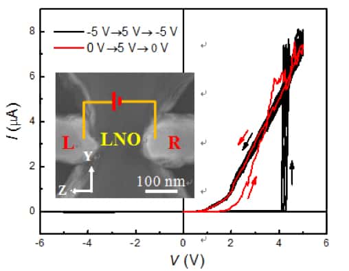
Led by Jun Jiang and An-Quan Jiang, the researchers used electron-beam lithography and dry etching processes to fabricate cells that were 60 nm high, 300 nm wide and 200 nm long on the surface of the LiNbO3. They then connected two left and right electrodes made from platinum (Pt) to opposite sides of a cell for subsequent measurements.
When they applied an electric field across the material via the electrodes, they observed that the domain within part of a cell reversed so that it pointed antiparallel to a domain at the bottom of the cell (which remained unswitched). This led to the formation of a conducting domain wall.
Interfacial “imprint field”
The team controlled the conducting domain wall’s current (which can be as high as 6 μA under an applied voltage of 4V) using two interfacial and unstable (volatile) domain walls that they connected to the two side Pt electrodes. The researchers explain that these interfacial domain walls then disappear, turning off the wall current path after the applied electric field has been removed or under a negative applied voltage.
Ferroelectric nematic appears in a liquid crystal
“We ascribe the rectifying behaviour to the volatile domains within the interfacial layers,” team member Chao Wang tells Physics World. “As we remove the applied voltage or reduce it to below the device’s onset voltage (Von), the interfacial domains switch back into their previous orientations thanks to the existence of an interfacial ‘imprint field’. This field does not exist in the bottom domain, which, as we remember, is non-volatile.”
Reporting its work in Chinese Physics Letters, the Fudan University team says it will now be focusing on optimizing the properties of its devices – namely their Von, their on/off current ratio and their stability.


